
Datasheet

AD9549
Rev. D | Page 24 of 76
The resulting loop filter coefficients for the lower loop
bandwidth, along with the necessary programming values,
are shown as follows:
α = 0.005883404361345
α
0
= 1542 (0x606)
α
1
= 0 (0x00)
α
2
= 7 (0x07)
β = −0.000003820176667
β
0
= 16 (0x10)
β
1
= 7 (0x07)
γ = −0.00000461136116
γ
0
= 19 (0x13)
γ
1
= 7 (0x07)
The AD9549 evaluation software generates these coefficients
automatically based on the user’s desired loop characteristics.
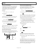
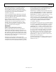
CLOSED-LOOP PHASE OFFSET
The AD9549 provides for limited control over the phase offset
between the reference input signal and the output signal by adding
a constant phase offset value to the output of the phase detector.
An adder is included at the output of the phase detector to support
this, as shown in Figure 28. The value of the constant (PLL
OFFSET
)
is set via the DPLL phase offset bits.
06744-028
PHASE
OFFSET
VALUE
PHASE
DETECTOR
LOOP
FILTER
TO CCI
FILTER
CLK
FEEDBACK
Figure 28. Input Phase Offset Adder
PLL
OFFSET
is a function of the phase detector gain and the
desired amount of timing offset (Δt
OFFSET
). It is given by
PLL
OFFSET
= Δt
OFFSET
(2
10
× 10
7
× FPFD_Gain
FPFD_Gain is described in the Fine Phase Detector section.
For example, suppose that FPFD_Gain = 200, f
CLK
= 3 MHz, and
1° of phase offset is desired. First, the value of Δt
OFFSET
must be
determined, as follows:
ps9.925
MHz3
1
360
1
360
deg
=
==∆
CLK
OFFSET
tt
Having determined Δt
OFFSET
,
1896)200102ps(9.925
710
=××=
OFFSET
PLL
The result has been rounded because PLL
OFFSET
is restricted to
integer values.
Note that the PLL
OFFSET
value is programmed as a 14-bit, twos
complement number. However, the user must ensure that the
magnitude is constrained to 12 bits, such that:
−2
11
≤ PLL
OFFSET
< +2
11
The preceding constraint yields a timing adjustment range of
±1 ns. This ensures that the phase offset remains within the
bounds of the fine phase detector.
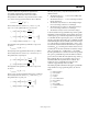
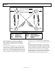
LOCK DETECTION
Phase Lock Detection
During the phase locking process, the output of the phase
detector tends toward a value of 0, which indicates perfect
alignment of the phase detector input signals. As the control
loop works to maintain the alignment of the phase detector
input signals, the output of the phase detector wanders around 0.
The phase lock detector tracks the absolute value of the digital
samples generated by the phase detector. These samples are
compared to the phase lock detect threshold value (PLDT)
programmed in the I/O register map. A false state at the output
of the comparator indicates that the absolute value of a sample
exceeds the value in the threshold bits. A true state at the output
of the comparator indicates alignment of the phase detector
input signals to the degree specified by the lock detection
threshold.
06744-029
ABSOLUTE
VALUE
DIGITAL
COMPARATOR
CONTROL LOGIC
UNLOCK
TIMER
LOCK
TIMER
PHASE LOCK DETECT
THRESHOLD
Y X CLOSE
LOOP
PHASE
LOCK
DETECT
RESET
P-DIVIDER
CLOCK
PHASE
DETECTOR
SAMPLES
I/O
REGISTERS
3 5
Figure 29. Phase Lock Detector Block Diagram
The phase lock detect threshold value is a 32-bit number stored
in the I/O register map.
( )
GainFPFDtPLDT _102round
710
×××∆=
where Δt is the maximum allowable timing error between the
signals at the input to the phase detector and the value of
FPFD_Gain is as described in the Fine Phase Detector section.
For example, suppose that f
R
/R = 3 MHz, FPFD_Gain = 200, and
the maximum timing deviation is given as 1°. This yields a Δt
value of
( )
)103(360
1
360360
1
6
×
==×
°
°
=∆
R
R
f
R
TRt
The resulting phase lock detect threshold is
1896
)103(360
200102
round
6
710
=
×
×
×
=PLDT
Hence, 1896 (0x00000768) is the value that must be stored in
the phase lock detect threshold bits.