
Datasheet


AD9553
Rev. A | Page 6 of 44
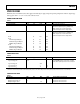
OUTPUT CHARACTERISTICS
Table 8.
Parameter Min Typ Max Unit Test Conditions/Comments
LVPECL MODE
Differential Output Voltage Swing 690 800 890 mV Output driver static (for dynamic performance, see
Figure 18)
Common-Mode Output Voltage VDD − 1.66 VDD − 1.34 VDD − 1.01 V Output driver static
Frequency Range 0 810 MHz
Duty Cycle 40 60 % Up to 805 MHz output frequency
Rise/Fall Time
1
(20% to 80%) 255 305 ps 100 Ω termination between both pins of the
output driver
LVDS MODE
Differential Output Voltage Swing Output driver static (for dynamic performance, see
Figure 18)
Balanced, V
OD
297 398 mV Voltage swing between the pins of a differential
output pair with the output driver static
Unbalanced, ΔV
OD
8.3 mV Absolute difference between voltage swing of
normal pin and inverted pin with the output
driver static
Offset Voltage
Common Mode, V
OS
1.17 1.35 V (V
OH
+ V
OL
)/2 across a differential pair with output
driver static
Common-Mode Difference, ΔV
OS
7.3 mV This is the absolute value of the difference
between V
OS
when the normal output is high vs.
when the complementary output is high with
output driver static
Short-Circuit Output Current 17 24 mA Output shorted to GND
Frequency Range 0 810 MHz
Duty Cycle 40 60 % Up to 805 MHz output frequency
Rise/Fall Time
1
(20% to 80%) 285 355 ps 100 Ω termination between both pins of the
output driver
CMOS MODE
Output Voltage High, V
OH
Output driver static; standard drive strength setting
I
OH
= 10 mA 2.8 V
I
OH
= 1 mA 2.8 V
Output Voltage Low, V
OL
Output driver static; standard drive strength setting
I
OL
= 10 mA 0.5 V
I
OL
= 1 mA 0.3 V
Frequency Range 0 200 MHz 3.3 V CMOS; standard drive strength setting;
output toggle rates in excess of the maximum are
possible, but with reduced amplitude (see Figure 17)
Duty Cycle 45 55 % At maximum output frequency
Rise/Fall Time
1
(20% to 80%) 500 745 ps 3.3 V CMOS; standard drive strength setting;
10 pF load
1
The listed values are for the slower edge (rise or fall).