Dual Input Multiservice Line Card Adaptive Clock Translator AD9557 Data Sheet FEATURES Pin program function for easy frequency translation configuration Software controlled power-down 40-lead, 6 mm × 6 mm, LFCSP package Supports GR-1244 Stratum 3 stability in holdover mode Supports smooth reference switchover with virtually no disturbance on output phase Supports Telcordia GR-253 jitter generation, transfer, and tolerance for SONET/SDH up to OC-192 systems Supports ITU-T G.
AD9557 Data Sheet TABLE OF CONTENTS Features .............................................................................................. 1 Digital PLL (DPLL) Core .......................................................... 30 Applications ....................................................................................... 1 Loop Control State Machine ..................................................... 32 General Description .......................................................................
Data Sheet AD9557 System Clock (Register 0x0100 to Register 0x0108) ..............66 General Configuration (Register 0x0200 to Register 0x0214) ..........................................................................67 Operational Controls (Register 0x0A00 to Register 0x0A0D) ........................................................................ 79 IRQ Mask (Register 0x020A to Register 0x020F) ...................68 Quick In/Out Frequency Soft Pin Configuration (Register 0x0C00 to Register 0x0C08) .
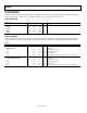
AD9557 Data Sheet SPECIFICATIONS Minimum (min) and maximum (max) values apply for the full range of supply voltage and operating temperature variations. Typical (typ) values apply for AVDD3 = DVDD_I/O = 3.3 V; AVDD = DVDD = 1.8 V; TA = 25°C, unless otherwise noted. SUPPLY VOLTAGE Table 1. Parameter SUPPLY VOLTAGE DVDD3 DVDD AVDD3 AVDD Min Typ Max Unit 3.135 1.71 3.135 1.71 3.30 1.80 3.30 1.80 3.465 1.89 3.465 1.
Data Sheet AD9557 POWER DISSIPATION Table 3. Parameter POWER DISSIPATION Typical Configuration Min Typ Max Unit Test Conditions/Comments 0.36 0.55 0.76 W All Blocks Running 0.39 0.61 0.85 W 44 125 mW System clock: 49.152 MHz crystal; DPLL active; both 19.44 MHz input references in differential mode; one HSTL driver at 644.53125 MHz; one 3.3 V CMOS driver at 161.1328125 MHz and 80 pF capacitive load on CMOS output System clock: 49.
AD9557 Data Sheet LOGIC OUTPUTS (M3 TO M0, IRQ) Table 5. Parameter LOGIC OUTPUTS (M3 to M0, IRQ) Output High Voltage (VOH) Output Low Voltage (VOL) IRQ Leakage Current Active Low Output Mode Active High Output Mode Min Typ Max Unit Test Conditions/Comments 0.4 V V −200 100 μA μA IOH = 1 mA IOL = 1 mA Open-drain mode VOH = 3.
Data Sheet AD9557 REFERENCE INPUTS Table 7. Parameter DIFFERENTIAL OPERATION Frequency Range Sinusoidal Input LVPECL Input LVDS Input Min Max Unit 10 0.002 750 1250 MHz MHz 0.
AD9557 Data Sheet REFERENCE MONITORS Table 8. Parameter REFERENCE MONITORS Reference Monitor Loss of Reference Detection Time Frequency Out-of Range Limits Validation Timer 1 Min Typ Max Unit Test Conditions/Comments 1.1 DPLL PFD period Δf/fREF (ppm) Nominal phase detector period = R/fREF 1 <2 105 0.001 65.
Data Sheet AD9557 DISTRIBUTION CLOCK OUTPUTS Table 10.
AD9557 Parameter OUTPUT TIMING SKEW Between OUT0 and OUT1 Data Sheet Typ Max Unit 10 70 ps −5 +1 +5 ps −5 0 +5 ps 3.53 3.
Data Sheet AD9557 DIGITAL PLL Table 12. Parameter DIGITAL PLL Phase-Frequency Detector (PFD) Input Frequency Range Loop Bandwidth Phase Margin Closed-Loop Peaking Reference Input (R) Division Factor Integer Feedback (N1) Division Factor Fractional Feedback Divide Ratio Min Typ Max Unit Test Conditions/Comments 2 100 kHz 0.1 30 <0.1 2000 89 Hz Degrees dB 1 180 0 220 217 0.
AD9557 Data Sheet SERIAL PORT SPECIFICATIONS—SPI MODE Table 15.
Data Sheet AD9557 SERIAL PORT SPECIFICATIONS—I2C MODE Table 16. Parameter SDA, SCL (AS INPUT) Input Logic 1 Voltage Min Typ 0.
AD9557 Parameter fREF = 19.44 MHz; fOUT = 644.53 MHz; fLOOP = 50 Hz HSTL and/or LVDS Driver Bandwidth: 5 kHz to 20 MHz Bandwidth: 12 kHz to 20 MHz Bandwidth: 20 kHz to 80 MHz Bandwidth: 50 kHz to 80 MHz Bandwidth: 16 MHz to 320 MHz fREF = 19.44 MHz; fOUT = 693.48 MHz; fLOOP = 50 Hz HSTL Driver Bandwidth: 5 kHz to 20 MHz Bandwidth: 12 kHz to 20 MHz Bandwidth: 20 kHz to 80 MHz Bandwidth: 50 kHz to 80 MHz Bandwidth: 16 MHz to 320 MHz fREF = 19.44 MHz; fOUT = 174.
Data Sheet AD9557 Jitter generation (random jitter) uses 19.2 MHz TCXO for system clock input. Table 18. Parameter JITTER GENERATION fREF = 19.44 MHz; fOUT = 644.53 MHz; fLOOP = 0.1 Hz HSTL Driver Bandwidth: 5 kHz to 20 MHz Bandwidth: 12 kHz to 20 MHz Bandwidth: 20 kHz to 80 MHz Bandwidth: 50 kHz to 80 MHz Bandwidth: 16 MHz to 320 MHz fREF = 19.44 MHz; fOUT = 693.48 MHz; fLOOP = 0.
AD9557 Data Sheet ABSOLUTE MAXIMUM RATINGS Table 19. Parameter Analog Supply Voltage (AVDD) Digital Supply Voltage (DVDD) Digital I/O Supply Voltage (DVDD3) Analog Supply Voltage (AVDD3) Maximum Digital Input Voltage Storage Temperature Range Operating Temperature Range Lead Temperature (Soldering 10 sec) Junction Temperature Rating 2V 2V 3.6 V 3.6 V −0.5 V to DVDD3 + 0.
Data Sheet AD9557 40 39 38 37 36 35 34 33 32 31 DVDD3 M3 M2 M1 M0 DVDD DVDD REFB REFB DVDD3 PIN CONFIGURATION AND FUNCTION DESCRIPTIONS PIN 1 INDICATOR AD9557 TOP VIEW (Not to Scale) 30 29 28 27 26 25 24 23 22 21 DVDD3 REFA REFA SYNC PINCONTROL RESET AVDD AVDD AVDD LF_VCO2 NOTES 1. THE EXPOSED PAD MUST BE CONNECTED TO GROUND (VSS).
AD9557 Data Sheet Pin No. 15 Mnemonic OUT0 Input/ Output O 16 OUT0 O 20 LDO_VCO2 I LDO bypass 21 LF_VCO2 I/O Loop filter RESET I 3.3 V CMOS PINCONTROL I 3.3 V CMOS SYNC I 3.3 V CMOS I Differential input I Differential input Power Differential input E 25 A E 26 A 27 E A REFA 28 29 REFA E 30, 31, 40 32 A Pin Type HSTL, LVDS, 1.8 V CMOS, 3.3 V CMOS HSTL, LVDS, 1.8 V CMOS, 3.3 V CMOS DVDD3 REFB I I REFB I 36, 37, 38, 39 M0, M1, M2, M3 I/O Differential input 3.
Data Sheet AD9557 TYPICAL PERFORMANCE CHARACTERISTICS fR = input reference clock frequency; fO = output clock frequency; fSYS = SYSCLK input frequency; fS = internal system clock frequency; LF = SYSCLK PLL internal loop filter used. AVDD, AVDD3, and DVDD at nominal supply voltage; fS = 786.432 MHz, unless otherwise noted.
AD9557 Data Sheet –60 –80 INTEGRATED RMS JITTER (12kHz TO 20MHz): 393fs INTEGRATED RMS JITTER (12kHz TO 20MHz): 302fs –70 –90 PHASE NOISE (dBc/Hz) PHASE NOISE (dBc/Hz) –80 –100 –110 –120 –130 –140 –90 –100 –110 –120 –130 –140 –150 1k 10k 100k 1M 10M 100M FREQUENCY OFFSET (Hz) –160 09197-007 –160 100 10 10k 100k 1M 10M 100M Figure 10. Absolute Phase Noise (Output Driver = HSTL), fR = 19.44 MHz, fO = 644.53 MHz, DPLL Loop BW = 0.1 Hz, fSYS = 19.
Data Sheet AD9557 DIFFERENTIAL PEAK-TO-PEAK AMPLITUDE (V) 10M 100M FREQUENCY OFFSET (Hz) 1.0 FREQUENCY (MHz) Figure 13. Absolute Phase Noise (Output Driver = 3.3 V CMOS), fR = 19.44 MHz, fO =161.1328125 MHz, DPLL Loop BW = 0.1 Hz, fSYS = 19.2 MHz TCXO Figure 16. Amplitude vs.
Data Sheet 70 3.0 60 2.5 50 2.0 1.5 30 20 0.5 10 0 10 20 30 40 50 60 70 80 FREQUENCY (MHz) 0 0 100 50 150 200 FREQUENCY (MHz) Figure 22. Power Consumption vs. Frequency, CMOS Mode on Output Driver Power Supply Only (Pin 11 and Pin 17) for 1.8 V CMOS Mode or on Pin 19 for 3.3 V CMOS Mode, One CMOS Driver Figure 19. Amplitude vs. Toggle Rate with 10 pF Load, 3.3 V (Weak Mode) CMOS 1.0 70 0.8 DIFFERENTIAL AMPLITUDE (V) 75 65 60 55 50 45 40 35 0.6 0.4 0.2 0 –0.2 –0.4 –0.6 –0.
Data Sheet AD9557 3 3.4 0 3.0 –3 2.6 LOOP GAIN (dB) 1.4 1.0 –9 –12 –15 –18 –21 2pF LOAD 10pF LOAD 0.6 0.2 0 1 2 3 4 5 6 7 8 TIME (ns) 9 10 11 12 13 14 15 Figure 25. Output Waveform, 3.3 V CMOS (100 MHz, Strong Mode) –27 LOOP BW = 5kHz; HIGH PHASE MARGIN; PEAKING: 0.14dB; –3dB: 4.27kHz 1.7 0 1.5 –3 LOOP GAIN (dB) 0.9 0.7 100k –9 –12 –15 –18 0.5 –21 2pF LOAD 10pF LOAD 0.3 LOOP BW = 100Hz; NORMAL PHASE MARGIN; PEAKING: 0.
AD9557 Data Sheet INPUT/OUTPUT TERMINATION RECOMMENDATIONS 10pF 0.1µF XOA XOB 10pF Figure 30. AC-Coupled LVDS or HSTL Output Driver (100 Ω resistor can go on either side of decoupling capacitors and should be as close as possible to the destination receiver.) Figure 33. System Clock Input (XOA, XOB) in Crystal Mode (The recommended CLOAD = 10 pF is shown. The values of the 10 pF shunt capacitors shown here should equal the CLOAD of the crystal.
Data Sheet AD9557 GETTING STARTED CHIP POWER MONITOR AND STARTUP The AD9557 monitors the voltage on the power supplies at power-up. When DVDD3 is greater than 2.35 V ± 0.1 V and DVDD and AVDD are greater than 1.4 V ± 0.05 V, the device generates a 20 ms reset pulse. The power-up reset pulse is internal and independent of the RESET pin. This internal power-up reset sequence eliminates the need for the user to provide external power supply sequencing.
AD9557 Data Sheet Program the System Clock and Free Run Tuning Word Program the Clock Distribution Outputs The system clock multiplier (SYSCLK) parameters are at Register 0x0100 to Register 0x0108, and the free run tuning word is at Register 0x0300 to Register 0x0303. Use the following steps for optimal performance: The APLL output goes to the clock distribution block. The clock distribution parameters reside in Register 0x0500 to Register 0x0509. They include the following: 1. 2. 3. 4. 5.
Data Sheet AD9557 Program the Digital Phase-Locked Loop (DPLL) Program the Reference Profiles The DPLL parameters reside in Register 0x0300 to Register 0x032E. They include the following: The reference profile parameters reside in Register 0x0700 to Register 0x0766. The AD9557 evaluation software contains a wizard that calculates these values based on the user’s input frequency. See the Reference Profiles section for details on programming these functions.
AD9557 Data Sheet THEORY OF OPERATION XO OR XTAL SPI/I2C SPI/I2C SERIAL PORT EEPROM RESET REGISTER SPACE PINCONTROL M0 M1 M2 M3 IRQ ROM AND FSM MULTIFUNCTION I/O PINS (CONTROL AND STATUS READBACK) SYSTEM CLOCK PLL XO FREQUENCIES 10MHz TO 180MHz XTAL: 10MHz TO 50MHz RF DIVIDER 1 ÷3 TO ÷11 ×2 ÷2 ÷M0 MAX 1.25GHz 2kHz TO 1.
Data Sheet AD9557 REFERENCE CLOCK INPUTS Reference Validation Timer Two pairs of pins provide access to the reference clock receivers. To accommodate input signals with slow rising and falling edges, both the differential and single-ended input receivers employ hysteresis. Hysteresis also ensures that a disconnected or floating input does not cause the receiver to oscillate. Each reference input has a dedicated validation timer.
AD9557 Data Sheet In the automatic modes, a fully automatic priority-based algorithm selects which reference is the active reference. When programmed for an automatic mode, the device chooses the highest priority valid reference. When both references have the same priority, REFA gets preference over REFB. However, the reference position is used only as a tie-breaker and does not initiate a reference switch. SYSTEM CLOCK • • • • • Automatic revertive mode.
Data Sheet AD9557 Programmable Digital Loop Filter The AD9557 loop filter is a third-order digital IIR filter that is analogous to the third-order analog loop shown in Figure 37. R2 C2 C3 Figure 37. Third Order Analog Loop Filter The AD9557 loop filter block features a simplified architecture in which the user enters the desired loop characteristics directly into the profile registers.
AD9557 Data Sheet During any given PFD cycle, the detector either adds water with the fill bucket or removes water with the drain bucket (one or the other but not both). The decision of whether to add or remove water depends on the threshold level specified by the user. The phase lock threshold value is a 16-bit number stored in the profile registers and is expressed in picoseconds (ps). Thus, the phase lock threshold extends from 0 ns to ±65.
Data Sheet AD9557 SYSTEM CLOCK (SYSCLK) SYSTEM CLOCK INPUTS Functional Description The SYSCLK circuit provides a low jitter, stable, high frequency clock for use by the rest of the chip. The XOA and XOB pins connect to the internal SYSCLK multiplier. The SYSCLK multiplier can synthesize the system clock by connecting a crystal resonator across the XOA and XOB input pins or by connecting a low frequency clock source.
AD9557 Data Sheet System Clock Stability Timer Because the reference monitors depend on the system clock being at a known frequency, it is important that the system clock be stable before activating the monitors. At initial powerup, the system clock status is not known, and, therefore, it is reported as being unstable. After the part has been programmed, the system clock PLL (if enabled) eventually locks.
Data Sheet AD9557 OUTPUT PLL (APLL) Calibration of the APLL must be performed at startup and whenever the nominal input frequency to the APLL changes by more than ±100 ppm, although the APLL maintains lock over voltage and temperature extremes without recalibration. Calibration centers the dc operating voltage at the input to the APLL VCO. A diagram of the output PLL (APLL) is shown in Figure 39. INTEGER DIVIDER ÷N2 OUTPUT PLL DIVIDER (APLL) PFD CP LF TO CLOCK DISTRIBUTION VCO2 3.35GHz TO 4.
AD9557 Data Sheet MAX 1.25GHz RF DIV 1 ÷3 TO ÷11 ÷M0 FROM DPLL (3.35GHz TO 4.05GHz) MAX 1.25GHz RF DIV 2 ÷3 TO ÷11 SYNC CHANNEL SYNC BLOCK 10-BIT INTEGER ÷M1 OUT0 OUT0 OUT1 OUT1 CHANNEL SYNC (TO M0 AND M1) 09197-139 CHIP RESET 10-BIT INTEGER 360kHz TO 1250MHz CLOCK DISTRIBUTION Figure 40. Clock Distribution Block Diagram A diagram of the clock distribution block appears in Figure 40.
Data Sheet AD9557 STATUS AND CONTROL MULTIFUNCTION PINS (M3 TO M0) The AD9557 has four digital CMOS I/O pins (M3 to M0) that are configurable for a variety of uses. To use these functions, the user must enable them by writing a 0x01 to Register 0x0200. The function of these pins is programmable via the register map. Each pin can control or monitor an assortment of internal functions, based on the contents of Register 0x0201 to Register 0x0204.
AD9557 Data Sheet If enabled, the timer runs continuously and generates a timeout event whenever the timeout period expires. The user has access to the watchdog timer status via the IRQ mechanism and the multifunction pins (M0 to M3). In the case of the multifunction pins, the timeout event of the watchdog timer is a pulse that lasts 32 system clock periods. There are two ways to reset the watchdog timer (thereby preventing it from causing a timeout event).
Data Sheet AD9557 Table 21. EEPROM Controller Instruction Set Instruction Value (Hex) 0x00 to 0x7F Instruction Type Data Bytes Required 3 0x80 I/O update 1 0xA0 Calibrate 1 0xA1 Distribution sync 1 0xB0 to 0xCF Condition 1 0xFE Pause 1 0xFF End 1 Description A data instruction tells the controller to transfer data to or from the device settings part of the register map. A data instruction requires two additional bytes that, together, indicate a starting address in the register map.
AD9557 Data Sheet A pause instruction, like an end instruction, is stored at the end of a sequence of instructions in the scratch pad. When the controller encounters a pause instruction during an upload sequence, it keeps the EEPROM address pointer at its last value. This way the user can store a new instruction sequence in the scratch pad and upload the new sequence to the EEPROM. The new sequence is stored in the EEPROM address locations immediately following the previously saved sequence.
Data Sheet AD9557 EEPROM Conditional Processing The condition tag board is a table maintained by the EEPROM controller. When the controller encounters a condition instructtion, it decodes the B1 through CF instructions as condition = 1 through condition = 8, respectively, and tags that particular condition in the condition tag board.
AD9557 Data Sheet Table 23 lists a sample EEPROM download instruction sequence. It illustrates the use of condition instructions and how they alter the download sequence. The table begins with the assumption that no conditions are in effect. That is, the most recently executed condition instruction is either B0 or no conditional instructions have been processed. Table 23.
Data Sheet The following changes write Register 0x0200 first and then issue an I/O update before writing the remaining M pin configuration registers in Register 0x0201 to Register 0x0208. The default EEPROM loading sequence from Register 0x0E10 to Register 0x0E16 is unchanged. The following steps must be inserted into the EEPROM storage sequence: 1. 2. 3. 4. 5. 6.
AD9557 Data Sheet SERIAL CONTROL PORT The AD9557 serial control port is a flexible, synchronous serial communications port that provides a convenient interface to many industry-standard microcontrollers and microprocessors. The serial control port is compatible with most synchronous transfer formats, including I²C, Motorola SPI, and Intel SSR protocols. The serial control port allows read/write access to the AD9557 register map. In SPI mode, single or multiple byte transfers are supported.
Data Sheet AD9557 Communication Cycle—Instruction Plus Data A readback operation takes data from either the serial control port buffer registers or the active registers, as determined by Register 0x0004, Bit 0. The SPI protocol consists of a two-part communication cycle. The first part is a 16-bit instruction word that is coincident with the first 16 SCLK rising edges and a payload. The instruction word provides the AD9557 serial control port with information regarding the payload.
AD9557 Data Sheet CS SCLK DON'T CARE R/W W1 W0 A12 A11 A10 A9 A8 A7 A6 A5 A4 A3 A2 A1 A0 D7 D6 D5 16-BIT INSTRUCTION HEADER D4 D3 D2 D1 D0 D7 D6 D5 REGISTER (N) DATA D4 D3 D2 DON'T CARE D1 D0 REGISTER (N – 1) DATA 09197-029 SDIO DON'T CARE DON'T CARE Figure 43.
Data Sheet AD9557 CS tS tC tCLK tHIGH tLOW tDS SCLK SDIO BIT N BIT N + 1 Figure 48. Serial Control Port Timing—Write Table 28.
AD9557 Data Sheet I2C SERIAL PORT OPERATION The transfer of data is shown in Figure 49. One clock pulse is generated for each data bit transferred. The data on the SDA line must be stable during the high period of the clock. The high or low state of the data line can change only when the clock signal on the SCL line is low. 2 The I C interface has the advantage of requiring only two control pins and is a de facto standard throughout the I2C industry.
Data Sheet AD9557 Data Transfer Process bytes immediately after the slave address byte are the internal memory (control registers) address bytes, with the high address byte first. This addressing scheme gives a memory address of up to 216 − 1 = 65,535. The data bytes after these two memory address bytes are register data written to or read from the control registers. In read mode, the data bytes after the slave address byte are register data written to or read from the control registers.
AD9557 Data Sheet Data Transfer Format Write byte format—the write byte protocol is used to write a register address to the RAM, starting from the specified RAM address. S Slave address A W E A RAM address high byte A RAM address low byte A RAM Data 0 A RAM Data 1 A RAM Data 2 A P Send byte format—the send byte protocol is used to set up the register address for subsequent reads.
Data Sheet AD9557 PROGRAMMING THE I/O REGISTERS REGISTER ACCESS RESTRICTIONS The register map spans an address range from 0x0000 through 0x0E3C. Each address provides access to 1 byte (eight bits) of data. Each individual register is identified by its four-digit hexadecimal address (for example, Register 0x0A10). In some cases, a group of addresses collectively defines a register.
AD9557 Data Sheet THERMAL PERFORMANCE Table 31. Thermal Parameters for the 40-Lead LFCSP Package Symbol θJA θJMA θJMA θJB θJC ΨJT 1 2 Thermal Characteristic Using a JEDEC51-7 Plus JEDEC51-5 2S2P Test Board1 Junction-to-ambient thermal resistance, 0.0 m/sec airflow per JEDEC JESD51-2 (still air) Junction-to-ambient thermal resistance, 1.0 m/sec airflow per JEDEC JESD51-6 (moving air) Junction-to-ambient thermal resistance, 2.
Data Sheet AD9557 POWER SUPPLY PARTITIONS The AD9557 power supplies are divided into four groups: DVDD3, DVDD, AVDD3, and AVDD. All power and ground pins should be connected, even if certain blocks of the chip are powered down. RECOMMENDED CONFIGURATION FOR 3.3 V SWITCHING SUPPLY A popular power supply arrangement is to power the AD9557 with the output of a 3.3 V switching power supply. The ADP7104 is another good choice for converting 3.3 V to 1.8 V.
AD9557 Data Sheet PIN PROGRAM FUNCTION DESCRIPTION The AD9557 supports both hard pin and soft pin program function, with the on-chip ROM containing the predefined configurations. When a pin program function is enabled and initiated, the selected, predefined configuration is transferred from the ROM to the corresponding registers to configure the part into the desired state.
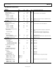
Data Sheet Freq ID 13 14 15 Frequency (MHz) 693.4830 698.8124 704.380580 AD9557 Hard Pin Program PINCONTROL = High M2 Pin M1 Pin M3 Pin ½ ½ ½ ½ ½ 1 ½ 1 0 Frequency Description 644.53125 MHz × 255/237 622.08 MHz × 255/237 657.421875 MHz × 255/238 B7 1 1 1 Soft Pin Program PINCONTROL = Low, Register 0x0C01[7:4] B6 B5 B4 1 0 1 1 1 0 1 1 1 Table 34. System Clock Configuration in Hard Pin and Soft Pin Programming Modes Freq ID 0 1 2 3 Frequency (MHz) 49.152 49.152 24.576 98.
AD9557 Data Sheet REGISTER MAP Register addresses that are not listed in Table 35 are not used, and writing to those registers has no effect. The user should write the default value to sections of registers marked reserved. R = read only. A = autoclear. E = excluded from EEPROM loading. L = live (I/O update not required for register to take effect or for a read-only register to be updated). Table 35.
Data Sheet Reg Addr (Hex) 0x0209 Opt 0x020A AD9557 Name IRQ pin output mode IRQ mask D7 D6 Reserved Reserved 0x020B D4 SYSCLK unlocked SYSCLK locked Pin program end Holdover Reserved 0x020C Switching 0x020D Closed Freerun Reserved 0x020E Reserved 0x020F 0x0210 0x0211 0x0300 0x0301 0x0302 0x0303 0x0304 Reserved Watchdog Timer 1 Free run frequency TW Digital oscillator control Reserved DPLL frequency clamp 0x0305 0x0306 0x0307 0x0308 0x0309 0x030A 0x030B 0x030C 0x030D 0x030E 0x030F 0x031
AD9557 Reg Addr Opt (Hex) 0x0323 L 0x0324 L 0x0325 L 0x0326 L 0x0327 L 0x0328 L 0x0329 L 0x032A L 0x032B L 0x032C L 0x032D L 0x032E L Output PLL (APLL) 0x0400 0x0401 0x0402 0x0403 0x0404 Data Sheet Name Base loop Filter A coefficient set (normal phase margin of 70º) D7 D3 D2 NPM Alpha-0[7:0] NPM Alpha-0[15:8] NPM Alpha-1[6:0] NPM Beta-0[7:0] NPM Beta-0[15:8] NPM Beta-1[6:0] NPM Gamma-0[7:0] NPM Gamma-0[15:8] NPM Gamma-1[6:0] NPM Delta-0[7:0] NPM Delta-0[15:8] NPM Delta-1[6:0] Reserved Reserved APLL c
Data Sheet Reg Addr Opt (Hex) Reference Inputs 0x0600 0x0601 0x0602 0x0603 Profile A (for REFA) 0x0700 L 0x0701 L 0x0702 L 0x0703 L 0x0704 L 0x0705 L 0x0706 L 0x0707 L 0x0708 L 0x0709 L 0x070A L 0x070B L 0x070C L 0x070D L 0x070E L AD9557 Name Reference powerdown Reference logic type Reference priority Reserved Reference period (up to 1.
AD9557 Reg Addr Opt (Hex) Profile B (for REFB) 0x0740 L 0x0741 L 0x0742 L 0x0743 L 0x0744 L 0x0745 L 0x0746 L 0x0747 L 0x0748 L 0x0749 L 0x074A L 0x074B L 0x074C L 0x074D L 0x074E L 0x074F 0x0750 0x0751 L L L 0x0752 0x0753 0x0754 L L L Data Sheet Name Reference period (up to 1.
Data Sheet Reg Addr (Hex) 0x0789 0x078A 0x078B 0x078C 0x078D 0x078E 0x078F 0x0790 0x0791 0x0792 0x0793 0x0794 0x0795 0x0796 0x0797 0x0798 0x0799 0x079A 0x079B 0x079C 0x079D 0x079E 0x079F 0x07A0 0x07A1 0x07A2 0x07A3 0x07A4 0x07A5 0x07A6 0x07C0 0x07C1 0x07C2 0x07C3 0x07C4 0x07C5 0x07C6 0x07C7 0x07C8 0x07C9 0x07CA 0x07CB 0x07CC 0x07CD 0x07CE 0x07CF 0x07D0 0x07D1 0x07D2 0x07D3 0x07D4 0x07D5 0x07D6 0x07D7 0x07D8 0x07D9 0x07DA Opt AD9557 Name D7 D6 D5 D4 0x07DB D3 Reserved Reserved Reserved Reserved Reser
AD9557 Data Sheet Reg Addr Opt Name (Hex) 0x07DC 0x07DD 0x07DE 0x07DF 0x07E0 0x07E1 0x07E2 0x07E3 0x07E4 0x07E5 0x07E6 Operational Controls 0x0A00 Power-down 0x0A01 Loop mode 0x0A02 Cal/sync 0x0A03 A 0x0A04 A 0x0A05 A 0x0A06 A 0x0A07 A 0x0A08 A 0x0A09 0x0A0A A A Clear/reset functions IRQ clearing D7 D6 D5 D4 D3 Reserved Reserved Reserved Reserved Reserved Reserved Reserved Reserved Reserved Reserved Reserved Soft reset exclude regmap Reserved DCO PD SYSCLK PD Ref input PD User
Data Sheet AD9557 Reg Addr Opt Name D7 D6 D5 (Hex) Read-Only Status (Accessible During EEPROM Transactions) 0x0D00 R, L EEPROM Reserved 0x0D01 R, L 0x0D02 R, L 0x0D03 R, L 0x0D04 R, L 0x0D05 R, L 0x0D06 R, L 0x0D07 R, L 0x0D08 R 0x0D09 R 0x0D0A 0x0D0B 0x0D0C 0x0D0D 0x0D0E 0x0D0F 0x0D10 0x0D11 0x0D12 R R R R R R R R R SYSCLK and PLL status IRQ monitor events Reserved A, E All PLLs locked SYSCLK unlocked Reserved Switching Closed Freerun Reserved Reserved REFB validated REFB fa
AD9557 Reg Addr Opt Name (Hex) EEPROM Storage Sequence 0x0E10 E EEPROM ID 0x0E11 E 0x0E12 E 0x0E13 E System clock 0x0E14 E 0x0E15 E 0x0E16 E I/O update 0x0E17 E General 0x0E18 E 0x0E19 E 0x0E1A E DPLL 0x0E1B E 0x0E1C E 0x0E1D E APLL 0x0E1E E 0x0E1F E 0x0E20 E Clock dist 0x0E21 E 0x0E22 E 0x0E23 E I/O update 0x0E24 E Reference inputs 0x0E25 E 0x0E26 E 0x0E27 E 0x0E28 E 0x0E29 E 0x0E2A E Profile REFA 0x0E2B E 0x0E2C E 0x0E2D E Profile REFB 0x0E2E E 0x0E2F E 0x0E30 E 0x0E31 E 0x0E32 E 0x0E33 E 0x0E34 E 0x0E35
Data Sheet AD9557 REGISTER MAP BIT DESCRIPTIONS SERIAL PORT CONFIGURATION (REGISTER 0x0000 TO REGISTER 0x0005) Table 36. Serial Configuration (Note that the contents of Register 0x0000 are not stored to the EEPROM.) Address 0x0000 Bits 7 Bit Name SDO enable 6 LSB first/increment address 5 Soft reset [4:0] Reserved Description Enables SPI port SDO pin. 1 = 4-wire (SDO pin enabled). 0 (default) = 3-wire. Bit order for SPI port. 1 = least significant bit and byte first.
AD9557 Data Sheet SYSTEM CLOCK (REGISTER 0x0100 TO REGISTER 0x0108) Table 42. System Clock PLL Feedback Divider (N3 Divider) Address 0x0100 Bits [7:0] Bit Name SYSCLK N3 divider Description System clock PLL feedback divider value: 4 ≤ N3 ≤ 255 (default: 0x08). Table 43. SYSCLK Configuration Address 0x0101 Bits [7:5] 4 Bit Name Reserved Load from ROM (read only) 3 SYSCLK XTAL enable [2:1] SYSCLK P divider 0 SYSCLK doubler enable Description Reserved.
Data Sheet AD9557 GENERAL CONFIGURATION (REGISTER 0x0200 TO REGISTER 0x0214) Multifunction Pin Control (M3 to M0) and IRQ Pin Control (Register 0x0200 to Register 0x0209) Note that the default setting for the M3 to M0 multifunction pins and the IRQ pin is that of a 3-level logic input at startup. Setting Bit 1 in Register 0x0200 to 1 enables normal M3 to M0 pin functionality. Table 46.
AD9557 Data Sheet IRQ MASK (REGISTER 0x020A TO REGISTER 0x020F) The IRQ mask register bits form a one-to-one correspondence with the bits of the IRQ monitor register (0x0D02 to 0x0D09). When set to Logic 1, the IRQ mask bits enable the corresponding IRQ monitor bits to indicate an IRQ event. The default for all IRQ mask bits is Logic 0, which prevents the IRQ monitor from detecting any internal interrupts. Table 48.
Data Sheet AD9557 Table 52.
AD9557 Data Sheet Table 56.
Data Sheet AD9557 Table 60. History Accumulation Timer Address 0x0314 Bits [7:0] 0x0315 [7:0] Bit Name History accumulation timer (ms) Description History accumulation timer bits[7:0]. Default: 0x0A. For Register 0x0314 and Register 0x0315, 0x000A = 10 ms. Maximum is 65 sec. This register controls the amount of tuning word averaging used to determine the tuning word used in holdover. Never program a timer value of zero. The default value is 0x000A = 10 decimal, which equates to 10 ms.
AD9557 Data Sheet Table 63. Base Digital Loop Filter with Normal Phase Margin (PM = 70°, BW = 0.
Data Sheet AD9557 Address Bits [2:0] Bit Name 0x0404 [7:1] 0 Reserved Bypass internal Rzero 0x0405 [7:4] 3 Reserved APLL locked controlled sync disable [2:1] 0 Reserved Manual APLL VCO calibration Description Pole 1 Cp1 Cp1 (pF) Bit 2 Bit 1 Bit 0 0 0 0 0 1 0 20 0 0 1 80 0 1 1 100 0 0 0 20 1 1 0 40 1 0 1 100 1 1 1 120 (default) 1 Default: 0x00 0 (default) = uses the internal Rzero resistor.
AD9557 Data Sheet OUTPUT CLOCK DISTRIBUTION (REGISTER 0x0500 TO REGISTER 0x0515) Table 67. Distribution Output Synchronization Settings Address 0x0500 Bits [7:6] 5 Bit Name Reserved Mask Channel 1 sync 4 Mask Channel 0 sync 3 2 Reserved Sync source selection [1:0] Automatic sync mode Description Reserved. Masks the synchronous reset to the Channel 1 divider. 0 (default) = unmasked. The output drivers do not toggle until a SYNC pulse occurs. 1 = masked.
Data Sheet AD9557 Table 69. Distribution Channel 0 Divider Setting Address 0x0502 Bits [7:0] Bit Name Channel 0 divider 0x0503 [7:4] 3 Reserved Channel 0 PD 2 Select RF divider for Channel 2 [1:0] [7:6] [5:0] Channel 0 divider Reserved Channel 0 divider phase 0x0504 Description 10-bit Channel 0 divider, Bits[7:0] (LSB). Division equals Channel 0 divider, Bits[9:0] + 1. ([9:0] = 0 is divide-by-1, [9:0] = 1 is divide-by-2…[9:0] = 1023 is divide-by-1024) Reserved 0 (default) = normal operation.
AD9557 Data Sheet REFERENCE INPUTS (REGISTER 0x0600 TO REGISTER 0x0602) Table 72. Reference Power-Down1 Address 0x0600 Bits [7:2] 1 Bit Name Reserved REFB power-down 0 REFA power-down Description Reserved. Powers down REFB input receiver. 0 (default) = not powered down. 1 = powered down. Powers down REFA input receiver. 0 (default) = not powered down. 1 = powered down. When all bits are set, the reference receiver section enters a deep sleep mode. 1 Table 73.
Data Sheet AD9557 DPLL PROFILE REGISTERS (REGISTER 0x0700 TO REGISTER 0x0766) Note that the default value of the REFA profile is as follows: input frequency = 19.44 MHz, output frequency = 622.08 MHz/155.52 MHz, loop bandwidth = 400 Hz, normal phase margin, inner tolerance = 5%, and outer tolerance = 10%. The default value of REFB profile is as follows: input frequency = 8 kHz, output frequency = 622.08 MHz/155.
AD9557 Data Sheet Table 80. DPLL Loop BW Scaling Factor—REFA Profile1 Address 0x070F 0x0710 Bits [7:0] [7:0] Bit Name DPLL loop BW scaling factor (unit of 0.1 Hz) 0x0711 [7:1] 0 Reserved BW scaling factor Description Digital PLL loop bandwidth scaling factor, Bits[7:0] (default: 0xF4). Digital PLL loop bandwidth scaling factor, Bits[15:8] (default: 0x01). The default for Register 0x070F to Register 0x0710 = 0x01F4 = 500 (50 Hz loop bandwidth.
Data Sheet AD9557 REFB Profile (Register 0x0740 to Register 0x0766) The REFB profile registers, Register 0x0740 to Register 0x0766, are identical to the REFA profile registers, Register 0x0700 to Register 0x0726. OPERATIONAL CONTROLS (REGISTER 0x0A00 TO REGISTER 0x0A0D) Table 86.
AD9557 Data Sheet Reset Functions (Register 0x0A03) Table 89. Reset Functions Address 0x0A03 (autoclear) Bits 7 6 5 4 3 2 1 Bit Name Reserved Clear LF Clear CCI Reserved Clear auto sync Clear TW history Clear all IRQs 0 Clear watchdog timer Description Default: 0b. Setting this bit clears the digital loop filter (intended as a debug tool). Setting this bit clears the CCI filter (intended as a debug tool). Default: 0b. Setting this bit resets the automatic synchronization logic (see Register 0x0500).
Data Sheet AD9557 Table 93. IRQ Clearing for History Update, Frequency Limit, and Phase Slew Limit Address 0x0A07 Bits [7:5] 4 3 2 1 0 Bit Name Reserved History updated Frequency unclamped Frequency clamped Phase slew unlimited Phase slew limited Description Reserved Clears history updated IRQ Clears frequency unclamped IRQ Clears frequency clamped IRQ Clears phase slew unlimited IRQ Clears phase slew limited IRQ Table 94.
AD9557 Data Sheet QUICK IN/OUT FREQUENCY SOFT PIN CONFIGURATION (REGISTER 0x0C00 TO REGISTER 0x0C08) Table 97.
Data Sheet Address 0x0C06 AD9557 Bits [7:5] 4 Bit Name Reserved Sel high PM base loop filter [3:2] DPLL loop BW [1:0] Reference input frequency tolerance 0x0C07 [7:1] 0 Reserved Soft pin start transfer 0x0C08 [7:1] 0 Reserved Soft pin reset Description Reserved 0 = base loop filter with normal (70°) phase margin (default). 1 = base loop filter with high (88.5°) phase margin. (<0.1 dB peaking in closed-loop transfer function). Scales the DPLL loop BW while in soft pin mode.
AD9557 Data Sheet IRQ Monitor (Register 0x0D02 to Register 0x0D07 If not masked via the IRQ mask registers (Register 0x0209 and Register 0x020A), the appropriate IRQ monitor bit is set to Logic 1 when the indicated event occurs. These bits are cleared only via the IRQ clearing registers (Register 0x0A04 to Register 0A0B), the reset all IRQs bit (Register 0x0A03[1]), or a device reset. Table 100.
Data Sheet AD9557 DPLL Status, Input Reference Status, Holdover History, and DPLL Lock Detect Tub Levels (Register 0x0D08 to Register 0x0D14) Table 105.
AD9557 Data Sheet Table 109. Digital PLL Lock Detect Tub Levels Address 0x0D11 0x0D12 0x0D13 0x0D14 Bits [7:0] [7:4] [3:0] [7:0] [7:4] [3:0] Bit Name Phase tub Frequency tub Reserved Frequency tub Description Read-only digital PLL lock detect bathtub level[7:0] (see the DPLL Frequency Lock Detector section). Reserved. Read-only digital PLL lock detect bathtub level[11:8] (see the DPLL Frequency Lock Detector section).
Data Sheet AD9557 Table 112. EEPROM Storage Sequence for General Configuration Settings Address 0x0E17 Bits [7:0] 0x0E18 [7:0] 0x0E19 [7:0] Bit Name General Description The default value of this register is 0x11, which the controller interprets as a data instruction. Its decimal value is 17, so this tells the controller to transfer 18 bytes of data (17 + 1), beginning at the address specified by the next two bytes. The controller stores 0x11 in the EEPROM and increments the EEPROM address pointer.
AD9557 Data Sheet Table 116. EEPROM Storage Sequence for Reference Input Settings Address 0x0E24 Bits [7:0] 0x0E25 [7:0] 0x0E26 [7:0] Bit Name Reference inputs Description The default value of this register is 0x03, which the controller interprets as a data instruction. Its decimal value is 3, so this tells the controller to transfer four bytes of data (3 + 1), beginning at the address specified by the next two bytes.
Data Sheet AD9557 Table 120. EEPROM Storage Sequence for Operational Control Settings Address 0x0E37 Bits [7:0] 0x0E38 [7:0] 0x0E39 [7:0] Bit Name Operational controls Description The default value of this register is 0x0D, which the controller interprets as a data instruction. Its decimal value is 13, so this tells the controller to transfer 14 bytes of data (13 + 1), beginning at the address specified by the next two bytes.
AD9557 Data Sheet Table 124.
Data Sheet AD9557 Table 125.
AD9557 Data Sheet OUTLINE DIMENSIONS 6.10 6.00 SQ 5.90 0.60 MAX 0.60 MAX 31 1 0.50 BSC 4.65 4.50 SQ 4.35 EXPOSED PAD (BOTTOM VIEW) 21 TOP VIEW 1.00 0.85 0.80 SEATING PLANE 12° MAX 0.50 0.40 0.30 0.80 MAX 0.65 TYP 0.30 0.23 0.18 0.05 MAX 0.02 NOM COPLANARITY 0.08 0.20 REF 10 20 11 0.25 MIN 4.50 REF FOR PROPER CONNECTION OF THE EXPOSED PAD, REFER TO THE PIN CONFIGURATION AND FUNCTION DESCRIPTIONS SECTION OF THIS DATA SHEET. COMPLIANT TO JEDEC STANDARDS MO-220-VJJD-2 06-04-2012-A 5.85 5.