
Datasheet


Data Sheet AD9557
Rev. B | Page 5 of 92
POWER DISSIPATION
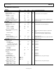
Table 3.
Parameter Min Typ Max Unit Test Conditions/Comments
POWER DISSIPATION
Typical Configuration 0.36 0.55 0.76 W System clock: 49.152 MHz crystal; DPLL active;
both 19.44 MHz input references in differential mode;
one HSTL driver at 644.53125 MHz;
one 3.3 V CMOS driver at 161.1328125 MHz and 80 pF
capacitive load on CMOS output
All Blocks Running 0.39 0.61 0.85 W System clock: 49.152 MHz crystal; DPLL active;
both input references in differential mode;
one HSTL driver at 750 MHz;
two 3.3 V CMOS drivers at 250 MHz and 80 pF capacitive
load on CMOS outputs
Full Power-Down
44
125
mW
Typical configuration with no external pull-up or pull-
down resistors; about 2/3 of this power is on AVDD3
Incremental Power Dissipation Conditions = typical configuration; table values show the
change in power due to the indicated operation
Input Reference On/Off
Differential Without Divide-by-2 20 25 32 mW Additional current draw is in the DVDD3 domain only
Differential With Divide-by-2 26 32 40 mW Additional current draw is in the DVDD3 domain only
Single-Ended Without Divide-by-2 5 7 9 mW Additional current draw is in the DVDD3 domain only
Output Distribution Driver On/Off
LVDS (at 750 MHz) 12 17 22 mW Additional current draw is in the AVDD domain only
HSTL (at 750 MHz) 14 21 28 mW Additional current draw is in the AVDD domain only
1.8 V CMOS (at 250 MHz) 14 21 28 mW A single 1.8 V CMOS output with an 80 pF load
3.3 V CMOS (at 250 MHz) 18 27 36 mW A single 3.3 V CMOS output with an 80 pF load
Other Blocks On/Off
Second RF Divider 36 51 64 mW Additional current draw is in the AVDD domain only
Channel Divider Bypassed 10 17 23 mW Additional current draw is in the AVDD domain only
LOGIC INPUTS (
RESET
,
SYNC
, PINCONTROL, M3 TO M0)
Table 4.
Parameter Min Typ Max Unit Test Conditions/Comments
LOGIC INPUTS (
E
A, A
SYNC
E
E
A, PINCONTROLA)
RESET
Input High Voltage (V
IH
) 2.1 V
Input Low Voltage (V
IL
) 0.8 V
Input Current (I
INH
, I
INL
) ±50 ±100 µA
Input Capacitance (C
IN
) 3 pF
LOGIC INPUTS (M3 to M0)
Input High Voltage (V
IH
)
2.5
V
Input ½ Level Voltage (V
IM
) 1.0 2.2 V
Input Low Voltage (V
IL
) 0.6 V
Input Current (I
INH
, I
INL
) ±60 ±100 µA
Input Capacitance (C
IN
) 3 pF