
Datasheet


Data Sheet AD9557
Rev. B | Page 9 of 92
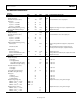
DISTRIBUTION CLOCK OUTPUTS
Table 10.
Parameter Min Typ Max Unit Test Conditions/Comments
HSTL MODE
Output Frequency 0.36 1250 MHz
Rise/Fall Time (20% to 80%)1F
1
140 250 ps 100 Ω termination across output pins
Duty Cycle
Up to f
OUT
= 700 MHz 45 48 52 %
Up to f
OUT
= 750 MHz 42 48 53 %
Up to f
OUT
= 1250 MHz 43 %
Differential Output Voltage Swing
700 950 1200 mV Magnitude of voltage across pins; output driver static
Common-Mode Output Voltage 700 870 960 mV Output driver static
LVDS MODE
Output Frequency 0.36 1250 MHz
Rise/Fall Time (20% to 80%)
1
185 280 ps 100 Ω termination across the output pair
Duty Cycle
Up to f
OUT
= 750 MHz 44 48 53 %
Up to f
OUT
= 800 MHz
43
47
53
%
Up to f
OUT
= 1250 MHz 43 %
Differential Output Voltage Swing
Balanced, V
OD
247 454 mV Voltage swing between output pins; output driver
static
Unbalanced, ΔV
OD
50 mV Absolute difference between voltage swing of
normal pin and inverted pin; output driver static
Offset Voltage
Common Mode, V
OS
1.125 1.26 1.375 V Output driver static
Common-Mode Difference, ΔV
OS
50 mV Voltage difference between pins; output driver static
Short-Circuit Output Current
13 24 mA Output driver static
CMOS MODE
Output Frequency
1.8 V Supply
0.36 150 MHz 10 pF load
3.3 V Supply (OUT0)
Strong Drive Strength Setting
0.36 250 MHz 10 pF load
Weak Drive Strength Setting
0.36 25 MHz 10 pF load
Rise/Fall Time(20% to 80%)
1
1.8 V Supply 1.5 3 ns 10 pF load
3.3 V Supply
Strong Drive Strength Setting 0.4 0.6 ns 10 pF load
Weak Drive Strength Setting
8 ns 10 pF load
Duty Cycle
1.8 V Mode
50 % 10 pF load
3.3 V Strong Mode
47 % 10 pF load
3.3 V Weak Mode 51 % 10 pF load
Output Voltage High (V
OH
) Output driver static; strong drive strength
AVDD3 = 3.3 V, I
OH
= 10 mA AVDD3 − 0.3 V
AVDD3 = 3.3 V, I
OH
= 1 mA AVDD3 − 0.1 V
AVDD3 = 1.8 V, I
OH
= 1 mA AVDD − 0.2 V
Output Voltage Low (V
OL
) Output driver static; strong drive strength
AVDD3 = 3.3 V, I
OL
= 10 mA 0.3 V
AVDD3 = 3.3 V, I
OL
= 1 mA 0.1 V
AVDD3 = 1.8 V, I
OL
= 1 mA 0.1 V