
Datasheet


AD9577 Data Sheet
Rev. 0 | Page 34 of 44
Integer Boundary Spurs
Another mechanism for fractional spur creation is the interactions
between the RF VCO frequency and the reference frequency.
When these frequencies are not integer related (the point of a
fractional-N synthesizer), spur sidebands appear on the VCO
output spectrum at an offset frequency that corresponds to the
beat note or difference frequency, between an integer multiple
of the reference and the VCO frequency. These spurs are attenuated
by the loop filter and are more noticeable on channels close to
integer multiples of the reference where the difference frequency
can be inside the loop bandwidth; therefore, the name integer
boundary spurs.
Reference Spurs
Reference spurs occur for both integer-N and fractional-N
operation. Reference spurs are generally not a problem in
fractional-N synthesizers because the reference offset is far
outside the loop bandwidth. However, any reference feed-
through mechanism that bypasses the loop may cause a problem.
Feedthrough of low levels of on-chip reference switching noise,
through the reference input or output pins back to the VCO, can
result in noticeable reference spur levels. In addition, coupling
of the reference frequency to the output clocks can result in beat
note spurs. PCB layout needs to ensure adequate isolation between
VCO/LDO supplies, the output traces, and the input or output
reference to avoid a possible feedthrough path on the board. If
the reference output clock (REFCLK) is not required, it should
be powered down to minimize potential board coupling. The
SDM digital circuitry is clocked by the reference clock. The
SDM is enabled when PLL2 is in fractional-N mode. When PLL2
is in fractional-N mode, the switching noise at the reference
frequency may result in increased spurs levels at the outputs.
OPTIMIZING PLL PERFORMANCE
Because the AD9577 can be configured in many ways, some guide-
lines should be followed to ensure that the high performance is
maintained. For both PLLs, there can be a small advantage in
choosing a lower VCO frequency because the VCO phase noise
tends to be slightly better at lower frequencies. Both VCOs should
not operate at the same frequency because this degrades jitter
performance. The two VCO frequencies should differ by at least
2 MHz. The following guidelines apply to PLL2 operating in
fractional-N mode only. If possible, denominators that have factors
of 2, 3, or 6 should be avoided because they can produce slightly
higher subfractional spur components. Avoid low and high
fractions (that is, FRAC/MOD close to 1/MOD or (MOD − 1)/
MOD) because these are more susceptible to larger fractional
spur components and integer boundary spurs. Avoid creating a
low valued beat frequency between the output frequency and the
PFD frequency to minimize the risk of low offset beat frequency
spurs. For example, setting f
PFD
= 25 MHz, and f
OUT
= 100.01 MHz
can create an output spur at 10 kHz offset to 100.01 MHz,
depending on board layout. Choosing a smaller MOD value results
in fractional spurs that are at a higher frequency and, consequently,
are better filtered by the PLL loop filter bandwidth of 50 kHz.
SETTING THE OUTPUT FREQUENCY OF PLL2
For example, to set the output frequency (f
OUT2
) on Port 2 to
155.52 MHz and the output frequency (f
OUT3
) on Port 3 to
38.88 MHz using a reference frequency (f
REF
) and PFD
frequency (f
PFD
) of 25 MHz, do the following.
The frequency f
OUT2
presented to OUT2 can be set according to
Equation 10.
The frequency f
OUT3
presented to OUT3 can be set according to
Equation 11.
In this case, both 155.52 MHz and 38.88 MHz can be derived
from the same VCO frequency because they are related by a
factor of 4.
The next step is to determine what the required values of f
VCO2
,
V2, and D2 are to divide down to 155.52 MHz. Table 24 shows
the available options.
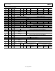
Table 24. Suitable Values of f
VCO2
and V2 × D2, to Achieve
f
OUT2
= 155.52 MHz
f
OUT2
(MHz) V2 × D2 f
VCO2
(GHz)
155.52 14 2.17728
155.52 15 2.3328
155.52 16 2.48832
Choose a f
VCO2
value of 2.48832 GHz. Next, determine that the
multiplication ratio (Nb + FRAC/MOD) required to multiply a
f
PFD
of 25 MHz up to 2.48832 GHz is 99.5328. Therefore, Nb must
be set to 99 and (FRAC/MOD) = 0.5328. To convert 0.5328 to a
fraction, 0.5328 can be the same as 5328/10000. This fraction
can then be reduced to the lowest terms by dividing both the
numerator and denominator by 16, where 16 is the greatest
common divisor (GCD) of the 5328 and 10,000. This results in
a solution for FRAC/MOD = 333/625.
For 155.52 MHz on Port 2, set V2 × D2 = 16. This can be achieved
by setting V2 to 4 and D2 to 4. For 38.88 MHz on Port 3, set V3
× D3 = 64. This can be achieved by setting V3 to 4 and D3 to
16. With a reference frequency of 25 MHz, the reference divider
value, R, must be set to 1 by setting Register G0[1] to 0. Because
both channels use VCO divide values of 4on V2 and V3, SyncCh23,
Register BDV2[0], can be set to 1 to ensure that the clock edges
on Port 2 and Port 3 are synchronized. Table 25 summarizes the
register setting for this configuration.
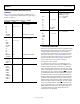
Table 25. Registers Setting for Example PLL2 Configuration
Parameter Value I
2
C Register Register Value
Nb 99 BF3[5:0] 010011
FRAC 333 BF0[7:0], BF1[7:4] 000101001101
MOD 625 BF1[3:0], BF2[7:0] 001001110001
V2 4 BDV0[7:5] 100
D2 4 BDV0[4:0] 00100
V3 4 BDV1[7:5] 100
D3 16 BDV1[4:0] 10000
R 1 G0[1] 0000
SyncCh23 1 BDV2[0] 1