
Datasheet


Table Of Contents
- FEATURES
- APPLICATIONS
- FUNCTIONAL BLOCK DIAGRAM
- PRODUCT HIGHLIGHTS
- TABLE OF CONTENTS
- REVISION HISTORY
- GENERAL DESCRIPTION
- SPECIFICATIONS
- ADC DC SPECIFICATIONS—AD9640ABCPZ-80, AD9640BCPZ80, AD9640ABCPZ-105, AND AD9640BCPZ-105
- ADC DC SPECIFICATIONS—AD9640ABCPZ-125, AD9640BCPZ125, AD9640ABCPZ-150, AND AD9640BCPZ150
- ADC AC SPECIFICATIONS—AD9640ABCPZ-80, AD9640BCPZ80, AD9640ABCPZ-105, AND AD9640BCPZ-105
- ADC AC SPECIFICATIONS—AD9640ABCPZ-125, AD9640BCPZ125, AD9640ABCPZ-150, AND AD9640BCPZ 150
- DIGITAL SPECIFICATIONS
- SWITCHING SPECIFICATIONS—AD9640ABCPZ-80, AD9640BCPZ-80, AD9640ABCPZ-105, AND AD9640BCPZ105
- SWITCHING SPECIFICATIONS—AD9640ABCPZ-125, AD9640BCPZ-125, AD9640ABCPZ-150, AND AD9640BCPZ150
- TIMING SPECIFICATIONS
- ABSOLUTE MAXIMUM RATINGS
- PIN CONFIGURATIONS AND FUNCTION DESCRIPTIONS
- EQUIVALENT CIRCUITS
- TYPICAL PERFORMANCE CHARACTERISTICS
- THEORY OF OPERATION
- ADC OVERRANGE AND GAIN CONTROL
- SIGNAL MONITOR
- BUILT-IN SELF-TEST (BIST) AND OUTPUT TEST
- CHANNEL/CHIP SYNCHRONIZATION
- SERIAL PORT INTERFACE (SPI)
- MEMORY MAP
- READING THE MEMORY MAP TABLE
- EXTERNAL MEMORY MAP
- MEMORY MAP REGISTER DESCRIPTION
- Sync Control (Register 0x100)
- Fast Detect Control (Register 0x104)
- Fine Upper Threshold (Register 0x106 and Register 0x107)
- Fine Lower Threshold (Register 0x108 and Register 0x109)
- Signal Monitor DC Correction Control (Register 0x10C)
- Signal Monitor DC Value Channel A (Register 0x10D and Register 0x10E)
- Signal Monitor DC Value Channel B (Register 0x10F and Register 0x110)
- Signal Monitor SPORT Control (Register 0x111)
- Signal Monitor Control (Register 0x112)
- Signal Monitor Period (Register 0x113 to Register 0x115)
- Signal Monitor Result Channel A (Register 0x116 to Register 0x118)
- Signal Monitor Result Channel B (Register 0x119 to Register 0x11B)
- APPLICATIONS INFORMATION
- OUTLINE DIMENSIONS
AD9640
Rev. B | Page 12 of 52
TIMING SPECIFICATIONS
Table 8.
Parameter Conditions Min Typ Max Unit
SYNC TIMING REQUIREMENTS
t
SSYNC
SYNC to rising edge of CLK setup time 0.24 ns
t
HSYNC
SYNC to rising edge of CLK hold time 0.40 ns
SPI TIMING REQUIREMENTS
t
DS
Setup time between the data and the rising edge of SCLK 2 ns
t
DH
Hold time between the data and the rising edge of SCLK 2 ns
t
CLK
Period of the SCLK 40 ns
t
S
Setup time between CSB and SCLK 2 ns
t
H
Hold time between CSB and SCLK 2 ns
t
HIGH
SCLK pulse width high 10 ns
t
LOW
SCLK pulse width low 10 ns
t
EN_SDIO
Time required for the SDIO pin to switch from an input to an
output relative to the SCLK falling edge
10 ns
t
DIS_SDIO
Time required for the SDIO pin to switch from an output to
an input relative to the SCLK rising edge
10 ns
SPORT TIMING REQUIREMENTS
t
CSSCLK
Delay from rising edge of CLK+ to rising edge of SMI SCLK 3.2 4.5 6.2 ns
t
SSCLKSDO
Delay from rising edge of SMI SCLK to SMI SDO −0.4 0 +0.4 ns
t
SSCLKSDFS
Delay from rising edge of SMI SCLK to SMI SDFS −0.4 0 +0.4 ns
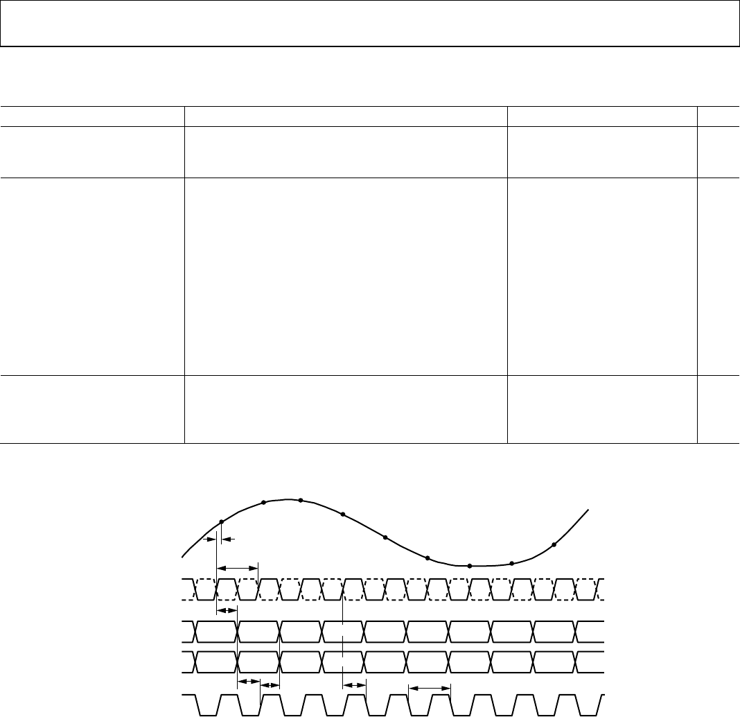
Timing Diagrams
CLK+
DCOA/DCOB
C
H A/B DAT
A
N
N+ 1
N+2
N+ 3
N+ 4
N+ 5
N+ 6
N+ 7
N+ 8
N – 12 N – 11 N – 9 N – 8 N – 7 N – 6 N – 5 N – 4
N – 13
CLK–
t
CLK
t
PD
t
S
t
H
t
DCO
t
CLK
t
A
CH A/B FAST
DETECT
N – 1 N + 2 N + 3 N + 4 N + 5 N + 6N – 3 N – 2
06547-021
N – 10
N + 1
N
Figure 2. CMOS Output Mode Data and Fast Detect Output Timing (Fast Detect Mode 0)