
Datasheet


Table Of Contents
- FEATURES
- APPLICATIONS
- FUNCTIONAL BLOCK DIAGRAM
- PRODUCT HIGHLIGHTS
- TABLE OF CONTENTS
- REVISION HISTORY
- GENERAL DESCRIPTION
- SPECIFICATIONS
- ADC DC SPECIFICATIONS—AD9640ABCPZ-80, AD9640BCPZ80, AD9640ABCPZ-105, AND AD9640BCPZ-105
- ADC DC SPECIFICATIONS—AD9640ABCPZ-125, AD9640BCPZ125, AD9640ABCPZ-150, AND AD9640BCPZ150
- ADC AC SPECIFICATIONS—AD9640ABCPZ-80, AD9640BCPZ80, AD9640ABCPZ-105, AND AD9640BCPZ-105
- ADC AC SPECIFICATIONS—AD9640ABCPZ-125, AD9640BCPZ125, AD9640ABCPZ-150, AND AD9640BCPZ 150
- DIGITAL SPECIFICATIONS
- SWITCHING SPECIFICATIONS—AD9640ABCPZ-80, AD9640BCPZ-80, AD9640ABCPZ-105, AND AD9640BCPZ105
- SWITCHING SPECIFICATIONS—AD9640ABCPZ-125, AD9640BCPZ-125, AD9640ABCPZ-150, AND AD9640BCPZ150
- TIMING SPECIFICATIONS
- ABSOLUTE MAXIMUM RATINGS
- PIN CONFIGURATIONS AND FUNCTION DESCRIPTIONS
- EQUIVALENT CIRCUITS
- TYPICAL PERFORMANCE CHARACTERISTICS
- THEORY OF OPERATION
- ADC OVERRANGE AND GAIN CONTROL
- SIGNAL MONITOR
- BUILT-IN SELF-TEST (BIST) AND OUTPUT TEST
- CHANNEL/CHIP SYNCHRONIZATION
- SERIAL PORT INTERFACE (SPI)
- MEMORY MAP
- READING THE MEMORY MAP TABLE
- EXTERNAL MEMORY MAP
- MEMORY MAP REGISTER DESCRIPTION
- Sync Control (Register 0x100)
- Fast Detect Control (Register 0x104)
- Fine Upper Threshold (Register 0x106 and Register 0x107)
- Fine Lower Threshold (Register 0x108 and Register 0x109)
- Signal Monitor DC Correction Control (Register 0x10C)
- Signal Monitor DC Value Channel A (Register 0x10D and Register 0x10E)
- Signal Monitor DC Value Channel B (Register 0x10F and Register 0x110)
- Signal Monitor SPORT Control (Register 0x111)
- Signal Monitor Control (Register 0x112)
- Signal Monitor Period (Register 0x113 to Register 0x115)
- Signal Monitor Result Channel A (Register 0x116 to Register 0x118)
- Signal Monitor Result Channel B (Register 0x119 to Register 0x11B)
- APPLICATIONS INFORMATION
- OUTLINE DIMENSIONS
AD9640
Rev. B | Page 17 of 52
PIN 1
INDICATOR
17
18
19
20
21
22
23
24
25
26
27
28
29
30
31
32
D7+
D8–
D8+
DRGND
DRVDD
D9–
D9+
DVDD
D10–
D10+
D11–
D11+
D12–
D12+
(MSB)
+ (MSB)
64
63
62
61
60
59
58
57
56
55
54
53
52
51
50
49
DRGND
D0+ (LSB)
D0– (LSB)
FD3+
FD3–
FD2+
FD2–
DVDD
FD1+
FD1–
FD0+
FD0–
SYNC
CSB
CLK–
CLK+
1
2
3
4
5
6
7
8
9
10
11
12
13
14
15
16
DRVDD
D1–
D1+
D2–
D2+
D3–
D3+
D4–
D4+
DCO–
DCO+
D5–
D5+
D6–
D6+
D7–
SCLK/DFS
SDIO/DCS
AVDD
AVDD
VIN+B
VIN–B
RBIAS
CML
SENSE
VREF
VIN–A
VIN+A
AVDD
SMI SDFS
SMI SCLK/PDWN
SMI SDO/OEB
48
47
46
45
44
43
42
41
40
39
38
37
36
35
34
33
D13–
D13
AD9640
PARALLEL LVDS
TOP VIEW
(Not to Scale)
EXPOSED PADDLE, PIN 0
(BOTTOM OF PACKAGE)
06547-003
NOTES
1. NC = NO CONNECT.
2. THE EXPOSED THERMAL PAD ON THE BOTTOM OF THE PACKAGE PROVIDES
THE ANALOG GROUND FOR THE PART. THIS EXPOSED PAD MUST BE
CONNECTED TO GROUND FOR PROPER OPERATION.
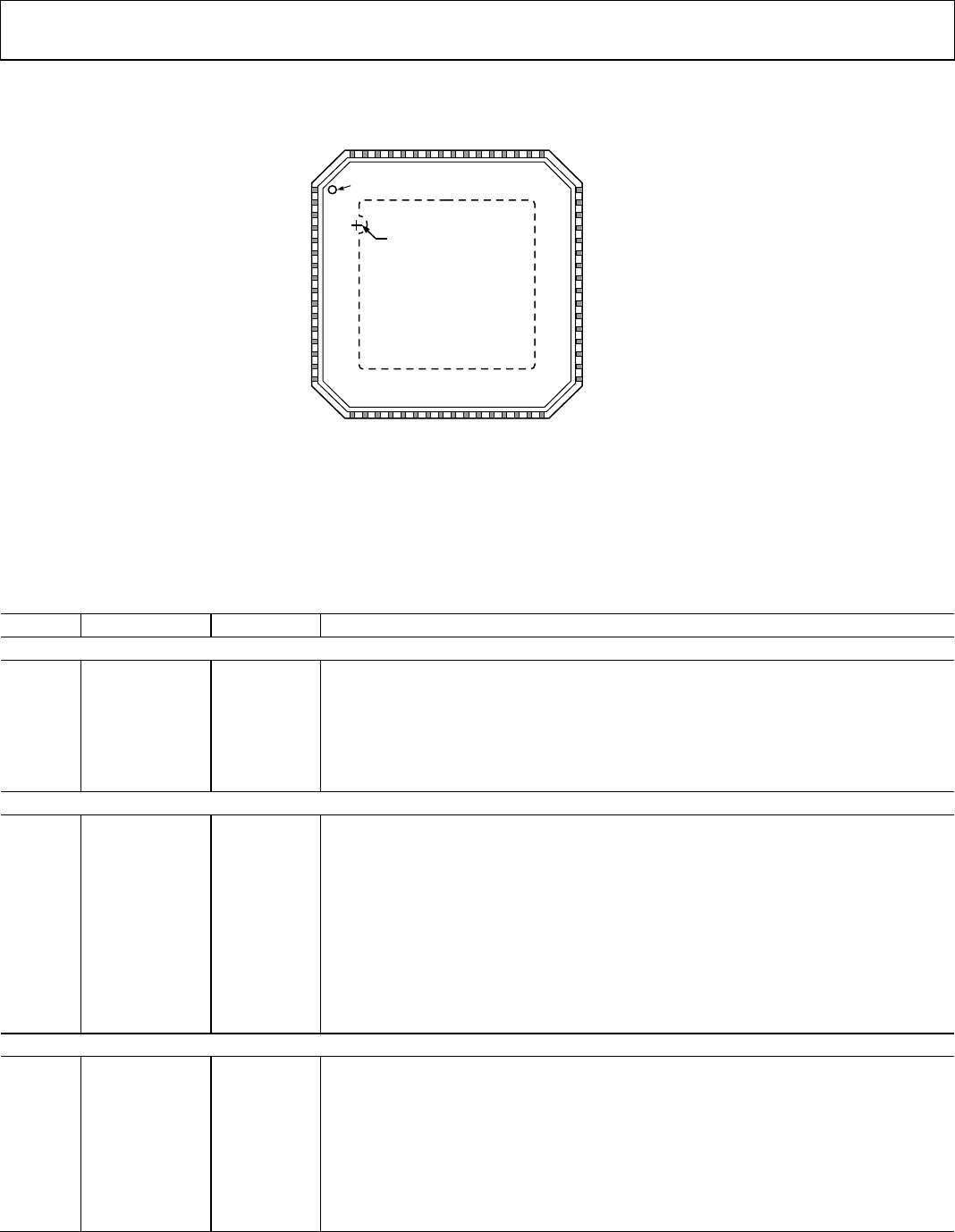
Figure 7. Pin Configuration, LFCSP LVDS (Top View)
Table 12. Pin Function Descriptions (Interleaved Parallel LVDS Mode)
Pin No. Mnemonic Type Function
ADC Power Supplies
20, 64 DRGND Ground Digital Output Ground.
1, 21 DRVDD Supply Digital Output Driver Supply (1.8 V to 3.3 V).
24, 57 DVDD Supply Digital Power Supply (1.8 V Nominal).
36, 45, 46 AVDD Supply Analog Power Supply (1.8 V Nominal).
0
AGND,
Exposed Pad
Ground
The exposed thermal pad on the bottom of the package provides the analog ground for the
part. This exposed pad must be connected to ground for proper operation.
ADC Analog
37 VIN+A Input Differential Analog Input Pin (+) for Channel A.
38 VIN−A Input Differential Analog Input Pin (−) for Channel A.
44 VIN+B Input Differential Analog Input Pin (+) for Channel B.
43 VIN−B Input Differential Analog Input Pin (−) for Channel B.
39 VREF Input/Output Voltage Reference Input/Output.
40 SENSE Input Voltage Reference Mode Select. See Table 14 for details.
42 RBIAS Input/Output External Reference Bias Resistor.
41 CML Output Common-Mode Level Bias Output for Analog Inputs.
49 CLK+ Input ADC Clock Input—True.
50 CLK− Input ADC Clock Input—Complement.
ADC Fast Detect Outputs
54 FD0+ Output Channel A/Channel B LVDS Fast Detect Indicator 0—True. See Table 18 for details.
53 FD0− Output Channel A/Channel B LVDS Fast Detect Indicator 0—Complement. See Table 18 for details.
56 FD1+ Output Channel A/Channel B LVDS Fast Detect Indicator 1—True. See Table 18 for details.
55 FD1− Output Channel A/Channel B LVDS Fast Detect Indicator 1—Complement. See Table 18 for details.
59 FD2+ Output Channel A/Channel B LVDS Fast Detect Indicator 2—True. See Table 18 for details.
58 FD2− Output Channel A/Channel B LVDS Fast Detect Indicator 2—Complement. See Table 18 for details.
61 FD3+ Output Channel A/Channel B LVDS Fast Detect Indicator 3—True. See Table 18 for details.
60 FD3− Output Channel A/Channel B LVDS Fast Detect Indicator 3—Complement. See Table 18 for details.