
Datasheet


Table Of Contents
- FEATURES
- APPLICATIONS
- FUNCTIONAL BLOCK DIAGRAM
- PRODUCT HIGHLIGHTS
- TABLE OF CONTENTS
- REVISION HISTORY
- GENERAL DESCRIPTION
- SPECIFICATIONS
- ADC DC SPECIFICATIONS—AD9640ABCPZ-80, AD9640BCPZ80, AD9640ABCPZ-105, AND AD9640BCPZ-105
- ADC DC SPECIFICATIONS—AD9640ABCPZ-125, AD9640BCPZ125, AD9640ABCPZ-150, AND AD9640BCPZ150
- ADC AC SPECIFICATIONS—AD9640ABCPZ-80, AD9640BCPZ80, AD9640ABCPZ-105, AND AD9640BCPZ-105
- ADC AC SPECIFICATIONS—AD9640ABCPZ-125, AD9640BCPZ125, AD9640ABCPZ-150, AND AD9640BCPZ 150
- DIGITAL SPECIFICATIONS
- SWITCHING SPECIFICATIONS—AD9640ABCPZ-80, AD9640BCPZ-80, AD9640ABCPZ-105, AND AD9640BCPZ105
- SWITCHING SPECIFICATIONS—AD9640ABCPZ-125, AD9640BCPZ-125, AD9640ABCPZ-150, AND AD9640BCPZ150
- TIMING SPECIFICATIONS
- ABSOLUTE MAXIMUM RATINGS
- PIN CONFIGURATIONS AND FUNCTION DESCRIPTIONS
- EQUIVALENT CIRCUITS
- TYPICAL PERFORMANCE CHARACTERISTICS
- THEORY OF OPERATION
- ADC OVERRANGE AND GAIN CONTROL
- SIGNAL MONITOR
- BUILT-IN SELF-TEST (BIST) AND OUTPUT TEST
- CHANNEL/CHIP SYNCHRONIZATION
- SERIAL PORT INTERFACE (SPI)
- MEMORY MAP
- READING THE MEMORY MAP TABLE
- EXTERNAL MEMORY MAP
- MEMORY MAP REGISTER DESCRIPTION
- Sync Control (Register 0x100)
- Fast Detect Control (Register 0x104)
- Fine Upper Threshold (Register 0x106 and Register 0x107)
- Fine Lower Threshold (Register 0x108 and Register 0x109)
- Signal Monitor DC Correction Control (Register 0x10C)
- Signal Monitor DC Value Channel A (Register 0x10D and Register 0x10E)
- Signal Monitor DC Value Channel B (Register 0x10F and Register 0x110)
- Signal Monitor SPORT Control (Register 0x111)
- Signal Monitor Control (Register 0x112)
- Signal Monitor Period (Register 0x113 to Register 0x115)
- Signal Monitor Result Channel A (Register 0x116 to Register 0x118)
- Signal Monitor Result Channel B (Register 0x119 to Register 0x11B)
- APPLICATIONS INFORMATION
- OUTLINE DIMENSIONS
AD9640
Rev. B | Page 25 of 52
THEORY OF OPERATION
The AD9640 dual ADC design can be used for diversity reception
of signals, where the ADCs are operating identically on the same
carrier but from two separate antennae. The ADCs can also be
operated with independent analog inputs. The user can sample
any f
S
/2 frequency segment from dc to 200 MHz using appropriate
low-pass or band-pass filtering at the ADC inputs with little loss
in ADC performance. Operation to 450 MHz analog input is
permitted but occurs at the expense of increased ADC distortion.
In nondiversity applications, the AD9640 can be used as a base-
band receiver, where one ADC is used for I input data and the
other is used for Q input data.
Synchronizaton capability is provided to allow synchronized
timing between multiple channels or multiple devices.
Programming and control of the AD9640 are accomplished
using a 3-bit SPI-compatible serial interface.
ADC ARCHITECTURE
The AD9640 architecture consists of a dual front-end sample-
and-hold amplifier (SHA), followed by a pipelined, switched
capacitor ADC. The quantized outputs from each stage are
combined into a final 14-bit result in the digital correction
logic. The pipelined architecture permits the first stage to
operate on a new input sample, and the remaining stages
operate on preceding samples. Sampling occurs on the rising
edge of the clock.
Each stage of the pipeline, excluding the last, consists of a low
resolution flash ADC connected to a switched capacitor digital-
to-analog converter (DAC) and an interstage residue amplifier
(MDAC). The residue amplifier magnifies the difference between
the reconstructed DAC output and the flash input for the next
stage in the pipeline. One bit of redundancy is used in each stage
to facilitate digital correction of flash errors. The last stage
simply consists of a flash ADC.
The input stage of each channel contains a differential SHA that
can be ac- or dc-coupled in differential or single-ended modes.
The output staging block aligns the data, carries out error correc-
tion, and passes the data to the output buffers. The output buffers
are powered from a separate supply, allowing adjustment of the
output voltage swing. During power-down, the output buffers go
into a high impedance state.
ANALOG INPUT CONSIDERATIONS
The analog input to the AD9640 is a differential switched
capacitor SHA that has been designed for optimum performance
while processing a differential input signal.
The clock signal alternatively switches the SHA between sample
mode and hold mode (see Figure 45). When the SHA is switched
into sample mode, the signal source must be capable of charging
the sample capacitors and settling within ½ of a clock cycle.
A small resistor in series with each input can help reduce the
peak transient current required from the output stage of the
driving source. A shunt capacitor can be placed across the
inputs to provide dynamic charging currents. This passive
network creates a low-pass filter at the ADC input; therefore,
the precise values are dependent on the application.
In intermediate frequency (IF) undersampling applications,
any shunt capacitors should be reduced. In combination with
the driving source impedance, they limit the input bandwidth.
See the AN-742 Application Note, Frequency Domain Response
of Switched-Capacitor ADCs; the AN-827 Application Note, A
Resonant Approach to Interfacing Amplifiers to Switched-Capacitor
ADCs; and the Analog Dialogue article, “Transformer-Coupled
Front-End for Wideband A/D Converters” for more information
on this subject.
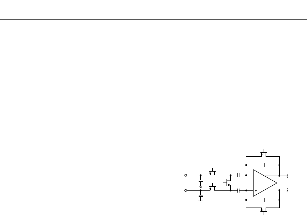
VIN+
VIN–
C
PIN, PAR
C
PIN, PAR
C
S
C
S
C
H
C
H
H
S
S
S
S
06547-024
Figure 45. Switched-Capacitor SHA Input
For best dynamic performance, the source impedances driving
VIN+ and VIN− should be matched.
An internal differential reference buffer creates positive and
negative reference voltages that define the input span of the ADC
core. The span of the ADC core is set by the buffer to 2 × VREF.
Input Common Mode
The analog inputs of the AD9640 are not internally dc biased.
In ac-coupled applications, the user must provide this bias
externally. Setting the device so that V
CM
= 0.55 × AVDD
is recommended for optimum performance, but the device
functions over a wider range with reasonable performance
(see Figure 44). An on-board common-mode voltage reference
is included in the design and is available from the CML pin.
Optimum performance is achieved when the common-mode
voltage of the analog input is set by the CML pin voltage
(typically 0.55 × AVDD). The CML pin must be decoupled to
ground by a 0.1 µF capacitor, as described in the Applications
Information section.
Differential Input Configurations
Optimum performance is achieved while driving the AD9640
in a differential input configuration. For baseband applications,
the AD8138 differential driver provides excellent performance
and a flexible interface to the ADC.