
Datasheet


Table Of Contents
- FEATURES
- APPLICATIONS
- FUNCTIONAL BLOCK DIAGRAM
- PRODUCT HIGHLIGHTS
- TABLE OF CONTENTS
- REVISION HISTORY
- GENERAL DESCRIPTION
- SPECIFICATIONS
- ADC DC SPECIFICATIONS—AD9640ABCPZ-80, AD9640BCPZ80, AD9640ABCPZ-105, AND AD9640BCPZ-105
- ADC DC SPECIFICATIONS—AD9640ABCPZ-125, AD9640BCPZ125, AD9640ABCPZ-150, AND AD9640BCPZ150
- ADC AC SPECIFICATIONS—AD9640ABCPZ-80, AD9640BCPZ80, AD9640ABCPZ-105, AND AD9640BCPZ-105
- ADC AC SPECIFICATIONS—AD9640ABCPZ-125, AD9640BCPZ125, AD9640ABCPZ-150, AND AD9640BCPZ 150
- DIGITAL SPECIFICATIONS
- SWITCHING SPECIFICATIONS—AD9640ABCPZ-80, AD9640BCPZ-80, AD9640ABCPZ-105, AND AD9640BCPZ105
- SWITCHING SPECIFICATIONS—AD9640ABCPZ-125, AD9640BCPZ-125, AD9640ABCPZ-150, AND AD9640BCPZ150
- TIMING SPECIFICATIONS
- ABSOLUTE MAXIMUM RATINGS
- PIN CONFIGURATIONS AND FUNCTION DESCRIPTIONS
- EQUIVALENT CIRCUITS
- TYPICAL PERFORMANCE CHARACTERISTICS
- THEORY OF OPERATION
- ADC OVERRANGE AND GAIN CONTROL
- SIGNAL MONITOR
- BUILT-IN SELF-TEST (BIST) AND OUTPUT TEST
- CHANNEL/CHIP SYNCHRONIZATION
- SERIAL PORT INTERFACE (SPI)
- MEMORY MAP
- READING THE MEMORY MAP TABLE
- EXTERNAL MEMORY MAP
- MEMORY MAP REGISTER DESCRIPTION
- Sync Control (Register 0x100)
- Fast Detect Control (Register 0x104)
- Fine Upper Threshold (Register 0x106 and Register 0x107)
- Fine Lower Threshold (Register 0x108 and Register 0x109)
- Signal Monitor DC Correction Control (Register 0x10C)
- Signal Monitor DC Value Channel A (Register 0x10D and Register 0x10E)
- Signal Monitor DC Value Channel B (Register 0x10F and Register 0x110)
- Signal Monitor SPORT Control (Register 0x111)
- Signal Monitor Control (Register 0x112)
- Signal Monitor Period (Register 0x113 to Register 0x115)
- Signal Monitor Result Channel A (Register 0x116 to Register 0x118)
- Signal Monitor Result Channel B (Register 0x119 to Register 0x11B)
- APPLICATIONS INFORMATION
- OUTLINE DIMENSIONS
AD9640
Rev. B | Page 26 of 52
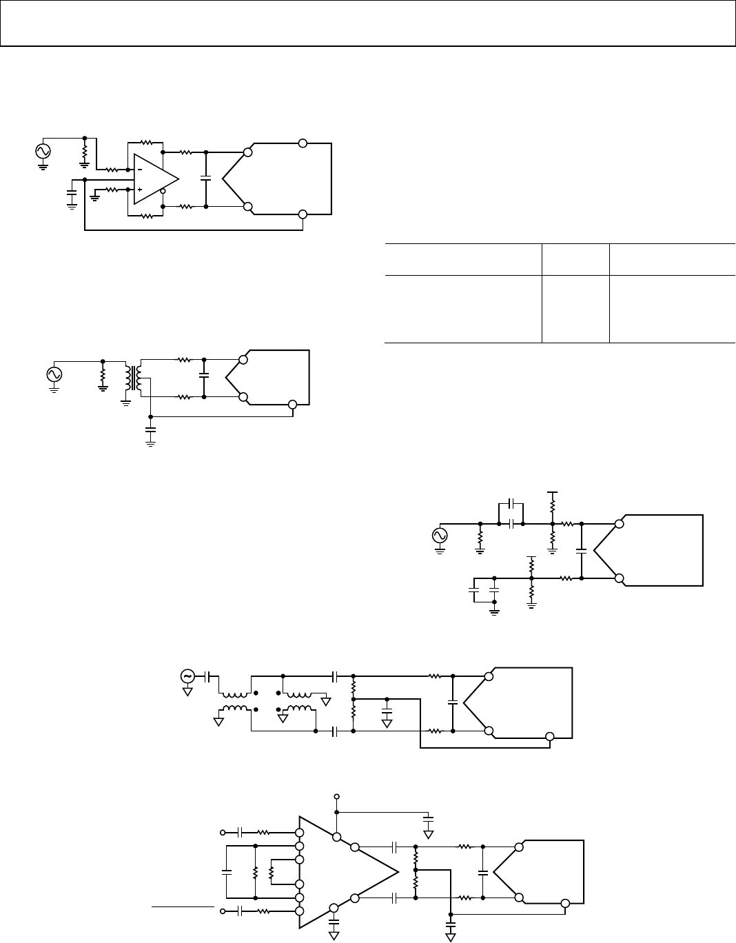
The output common-mode voltage of the AD8138 is easily set
with the CML pin of the AD9640 (see Figure 46), and the driver
can be configured in a Sallen-Key filter topology to provide
band limiting of the input signal.
AVDD
1V p-p
49.9Ω
523Ω
0.1µF
R
R
C
499Ω
499Ω
499Ω
AD8138
06547-025
AD9640
VIN+
VIN–
CML
Figure 46. Differential Input Configuration Using the AD8138
For baseband applications where SNR is a key parameter,
differential transformer coupling is the recommended input
configuration. An example is shown in Figure 47. To bias the
analog input, the CML voltage can be connected to the center
tap of the transformer’s secondary winding.
2V p-p
49.9Ω
0.1µF
R
R
C
06547-026
AD9640
VIN+
VIN–
CML
Figure 47. Differential Transformer-Coupled Configuration
The signal characteristics must be considered when selecting
a transformer. Most RF transformers saturate at frequencies
below a few MHz, and excessive signal power can also cause
core saturation, which leads to distortion.
At input frequencies in the second Nyquist zone and above, the
noise performance of most amplifiers is not adequate to achieve
the true SNR performance of the AD9640. For applications where
SNR is a key parameter, differential double balun coupling is the
recommended input configuration (see Figure 49 for an example).
An alternative to using a transformer coupled input at frequencies
in the second Nyquist zone is to use the AD8352 differential
driver. An example is shown in Figure 50. See the AD8352 data
sheet for more information.
In any configuration, the value of Shunt Capacitor C is dependent
on the input frequency and source impedance and may need to
be reduced or removed. Table 13 displays recommended values to
set the RC network. However, these values are dependent on the
input signal and should be used only as a starting guide.
Table 13. Example RC Network
Frequency Range (MHz)
R Series
(Ω Each) C Differential (pF)
0 to 70 33 15
70 to 200 33 5
200 to 300 15 5
>300 15 Open
Single-Ended Input Configuration
A single-ended input can provide adequate performance in cost
sensitive applications. In this configuration, SFDR and distortion
performance degrade due to the large input common-mode swing.
If the source impedances on each input are matched, there should
be little effect on SNR performance. Figure 48 details a typical
single-ended input configuration.
1V p-p
R
R
C
49.9Ω
0.1µF
10µF
10µF
0.1µF
AVDD
1kΩ
1kΩ
1kΩ
1kΩ
AD9640
A
V
DD
06547-071
VIN+
VIN–
Figure 48. Single-Ended Input Configuration
AD9640
R
0.1µF
0.1µF
2V p-p
VIN+
VIN–
CML
C
R
0.1µF
S
0.1µF
06547-028
25Ω
25Ω
SP
A
P
Figure 49. Differential Double Balun Input Configuration
AD9640
AD8352
0Ω
R
0Ω
C
D
R
D
R
G
0.1µF
0.1µF
0.1µF
VIN+
VIN–
CML
C
0.1µF
16
1
2
3
4
5
11
R
0.1µF
0.1µF
10
14
0.1µF
8, 13
V
CC
200Ω
200Ω
06547-070
ANALOG INPUT
ANALOG INPUT
Figure 50. Differential Input Configuration Using the AD8352