
Datasheet


Table Of Contents
- FEATURES
- APPLICATIONS
- FUNCTIONAL BLOCK DIAGRAM
- PRODUCT HIGHLIGHTS
- TABLE OF CONTENTS
- REVISION HISTORY
- GENERAL DESCRIPTION
- SPECIFICATIONS
- ADC DC SPECIFICATIONS—AD9640ABCPZ-80, AD9640BCPZ80, AD9640ABCPZ-105, AND AD9640BCPZ-105
- ADC DC SPECIFICATIONS—AD9640ABCPZ-125, AD9640BCPZ125, AD9640ABCPZ-150, AND AD9640BCPZ150
- ADC AC SPECIFICATIONS—AD9640ABCPZ-80, AD9640BCPZ80, AD9640ABCPZ-105, AND AD9640BCPZ-105
- ADC AC SPECIFICATIONS—AD9640ABCPZ-125, AD9640BCPZ125, AD9640ABCPZ-150, AND AD9640BCPZ 150
- DIGITAL SPECIFICATIONS
- SWITCHING SPECIFICATIONS—AD9640ABCPZ-80, AD9640BCPZ-80, AD9640ABCPZ-105, AND AD9640BCPZ105
- SWITCHING SPECIFICATIONS—AD9640ABCPZ-125, AD9640BCPZ-125, AD9640ABCPZ-150, AND AD9640BCPZ150
- TIMING SPECIFICATIONS
- ABSOLUTE MAXIMUM RATINGS
- PIN CONFIGURATIONS AND FUNCTION DESCRIPTIONS
- EQUIVALENT CIRCUITS
- TYPICAL PERFORMANCE CHARACTERISTICS
- THEORY OF OPERATION
- ADC OVERRANGE AND GAIN CONTROL
- SIGNAL MONITOR
- BUILT-IN SELF-TEST (BIST) AND OUTPUT TEST
- CHANNEL/CHIP SYNCHRONIZATION
- SERIAL PORT INTERFACE (SPI)
- MEMORY MAP
- READING THE MEMORY MAP TABLE
- EXTERNAL MEMORY MAP
- MEMORY MAP REGISTER DESCRIPTION
- Sync Control (Register 0x100)
- Fast Detect Control (Register 0x104)
- Fine Upper Threshold (Register 0x106 and Register 0x107)
- Fine Lower Threshold (Register 0x108 and Register 0x109)
- Signal Monitor DC Correction Control (Register 0x10C)
- Signal Monitor DC Value Channel A (Register 0x10D and Register 0x10E)
- Signal Monitor DC Value Channel B (Register 0x10F and Register 0x110)
- Signal Monitor SPORT Control (Register 0x111)
- Signal Monitor Control (Register 0x112)
- Signal Monitor Period (Register 0x113 to Register 0x115)
- Signal Monitor Result Channel A (Register 0x116 to Register 0x118)
- Signal Monitor Result Channel B (Register 0x119 to Register 0x11B)
- APPLICATIONS INFORMATION
- OUTLINE DIMENSIONS
AD9640
Rev. B | Page 27 of 52
VOLTAGE REFERENCE
A stable and accurate voltage reference is built into the AD9640.
The input range can be adjusted by varying the reference voltage
applied to the AD9640, using either the internal reference or an
externally applied reference voltage. The input span of the ADC
tracks reference voltage changes linearly. The various reference
modes are summarized in the next few sections. The Reference
Decoupling section describes the best practices PCB layout of
the reference.
Internal Reference Connection
A comparator within the AD9640 detects the potential at the
SENSE pin and configures the reference into four possible
modes, which are summarized in Table 14. If SENSE is grounded,
the reference amplifier switch is connected to the internal
resistor divider (see Figure 51), setting VREF to 1 V. Connecting
the SENSE pin to VREF switches the reference amplifier output
to the SENSE pin, completing the loop and providing a 0.5 V
reference output. If a resistor divider is connected external to
the chip, as shown in Figure 52, the switch again sets to the
SENSE pin. This puts the reference amplifier in a noninverting
mode with the VREF output defined as
⎟
⎠
⎞
⎜
⎝
⎛
+×=
R1
R2
VREF 15.0
The input range of the ADC always equals twice the voltage at
the reference pin for either an internal or an external reference.
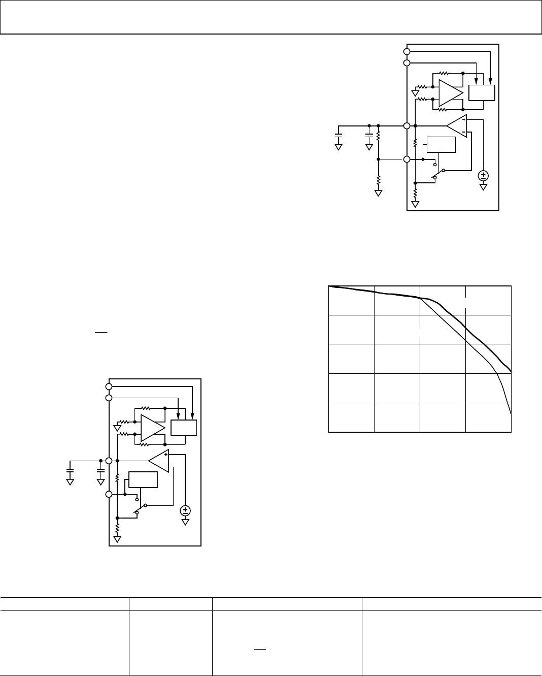
VREF
SENSE
0.5V
AD9640
SELECT
LOGIC
0.1µF1.0µF
06547-030
VIN–A/VIN–B
VIN+A/VIN+B
ADC
CORE
Figure 51. Internal Reference Configuration
0.5V
AD9640
SELECT
LOGIC
06547-031
VIN–A/VIN–B
VIN+A/VIN+B
ADC
CORE
VREF
SENSE
0.1µF1.0µF
R2
R1
Figure 52. Programmable Reference Configuration
If the internal reference of the AD9640 is used to drive multiple
converters to improve gain matching, the loading of the reference
by the other converters must be considered. Figure 53 shows
how the internal reference voltage is affected by loading.
0
–1.25
02
LOAD CURRENT (mA)
REFERENCE VOLTAGE ERROR (%)
.0
–0.25
–0.50
–0.75
–1.00
0.5 1.0 1.5
VREF = 0.5V
VREF = 1V
06547-080
Figure 53. VREF Accuracy vs. Load
External Reference Operation
The use of an external reference may be necessary to enhance
the gain accuracy of the ADC or improve thermal drift charac-
teristics. Figure 54 shows the typical drift characteristics of the
internal reference in 1 V mode.
Table 14. Reference Configuration Summary
Selected Mode SENSE Voltage Resulting VREF (V) Resulting Differential Span (V p-p)
External Reference AVDD N/A 2 × External Reference
Internal Fixed Reference VREF 0.5 1.0
Programmable Reference 0.2 V to VREF
⎟
⎠
⎞
⎜
⎝
⎛
+×
R1
R2
15.0
(see Figure 52)
2 × VREF
Internal Fixed Reference AGND to 0.2 V 1.0 2.0