
Datasheet


Table Of Contents
- FEATURES
- APPLICATIONS
- FUNCTIONAL BLOCK DIAGRAM
- PRODUCT HIGHLIGHTS
- TABLE OF CONTENTS
- REVISION HISTORY
- GENERAL DESCRIPTION
- SPECIFICATIONS
- ADC DC SPECIFICATIONS—AD9640ABCPZ-80, AD9640BCPZ80, AD9640ABCPZ-105, AND AD9640BCPZ-105
- ADC DC SPECIFICATIONS—AD9640ABCPZ-125, AD9640BCPZ125, AD9640ABCPZ-150, AND AD9640BCPZ150
- ADC AC SPECIFICATIONS—AD9640ABCPZ-80, AD9640BCPZ80, AD9640ABCPZ-105, AND AD9640BCPZ-105
- ADC AC SPECIFICATIONS—AD9640ABCPZ-125, AD9640BCPZ125, AD9640ABCPZ-150, AND AD9640BCPZ 150
- DIGITAL SPECIFICATIONS
- SWITCHING SPECIFICATIONS—AD9640ABCPZ-80, AD9640BCPZ-80, AD9640ABCPZ-105, AND AD9640BCPZ105
- SWITCHING SPECIFICATIONS—AD9640ABCPZ-125, AD9640BCPZ-125, AD9640ABCPZ-150, AND AD9640BCPZ150
- TIMING SPECIFICATIONS
- ABSOLUTE MAXIMUM RATINGS
- PIN CONFIGURATIONS AND FUNCTION DESCRIPTIONS
- EQUIVALENT CIRCUITS
- TYPICAL PERFORMANCE CHARACTERISTICS
- THEORY OF OPERATION
- ADC OVERRANGE AND GAIN CONTROL
- SIGNAL MONITOR
- BUILT-IN SELF-TEST (BIST) AND OUTPUT TEST
- CHANNEL/CHIP SYNCHRONIZATION
- SERIAL PORT INTERFACE (SPI)
- MEMORY MAP
- READING THE MEMORY MAP TABLE
- EXTERNAL MEMORY MAP
- MEMORY MAP REGISTER DESCRIPTION
- Sync Control (Register 0x100)
- Fast Detect Control (Register 0x104)
- Fine Upper Threshold (Register 0x106 and Register 0x107)
- Fine Lower Threshold (Register 0x108 and Register 0x109)
- Signal Monitor DC Correction Control (Register 0x10C)
- Signal Monitor DC Value Channel A (Register 0x10D and Register 0x10E)
- Signal Monitor DC Value Channel B (Register 0x10F and Register 0x110)
- Signal Monitor SPORT Control (Register 0x111)
- Signal Monitor Control (Register 0x112)
- Signal Monitor Period (Register 0x113 to Register 0x115)
- Signal Monitor Result Channel A (Register 0x116 to Register 0x118)
- Signal Monitor Result Channel B (Register 0x119 to Register 0x11B)
- APPLICATIONS INFORMATION
- OUTLINE DIMENSIONS
AD9640
Rev. B | Page 28 of 52
2.5
–2.5
–40
06547-099
TEMPERATURE (°C)
REFERENCE VOLTAGE ERROR (mV)
2.0
1.5
1.0
0
–0.5
–1.0
–1.5
–2.0
–200 20406080
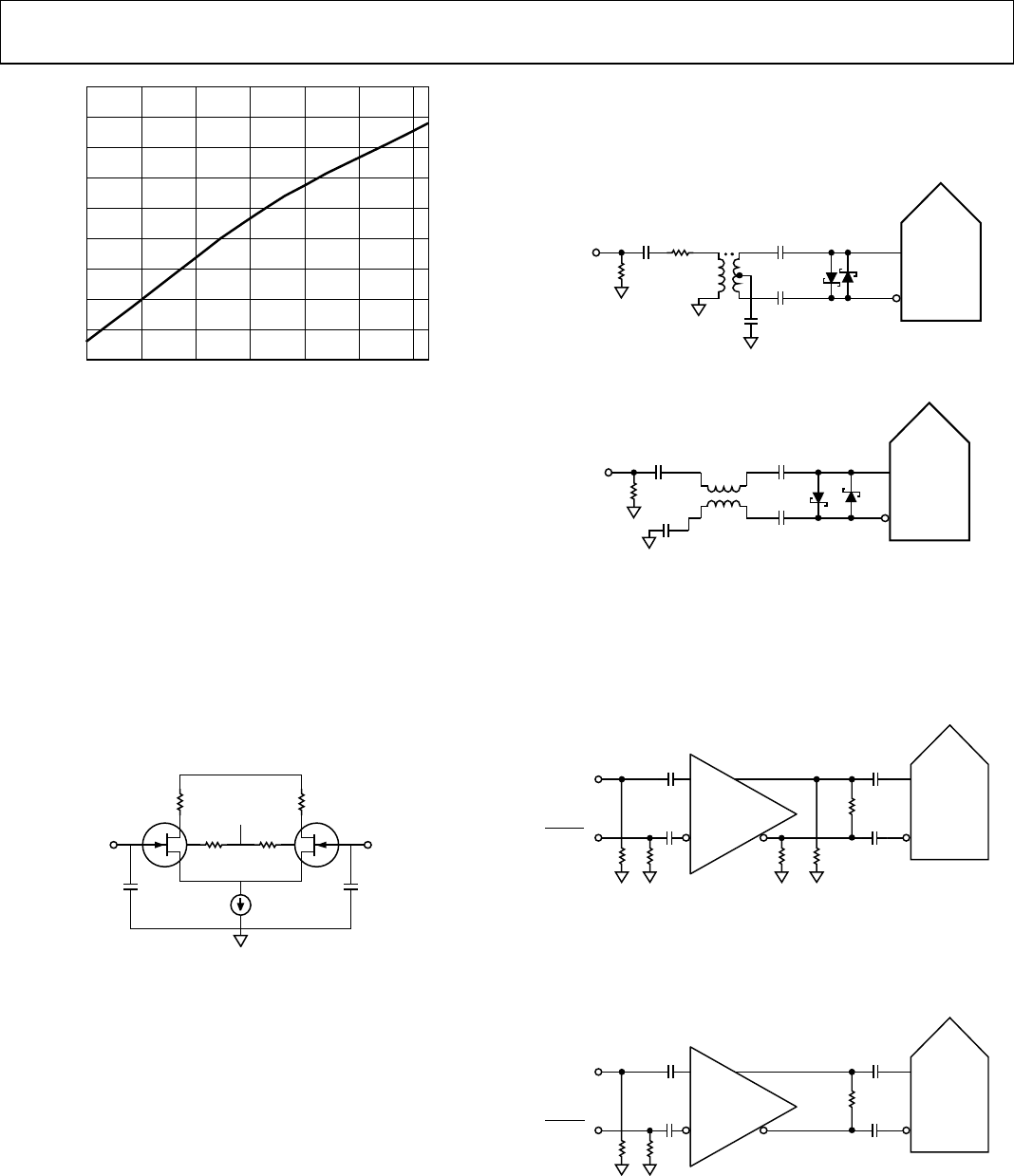
Figure 54. Typical VREF Drift
When the SENSE pin is tied to AVDD, the internal reference is
disabled, allowing the use of an external reference. An internal
reference buffer loads the external reference with an equivalent
6 kΩ load (see Figure 15). The internal buffer generates the
positive and negative full-scale references for the ADC core.
Therefore, the external reference must be limited to a maximum
of 1 V.
CLOCK INPUT CONSIDERATIONS
For optimum performance, the AD9640 sample clock inputs
CLK+, and CLK− should be clocked with a differential signal.
The signal is typically ac-coupled into the CLK+ and CLK− pins
via a transformer or capacitors. These pins are biased internally
(see Figure 55) and require no external bias.
0
6547-034
1.2V
A
V
DD
2pF 2pF
CLK–CLK+
Figure 55. Equivalent Clock Input Circuit
Clock Input Options
The AD9640 has a very flexible clock input structure. Clock input
can be a CMOS, LVDS, LVPECL, or sine wave signal. Regardless of
the type of signal being used, the jitter of the clock source is of the
most concern, as described in the Jitter Considerations section.
Figure 56 and Figure 57 show two preferred methods for clocking
the AD9640 (at clock rates to 625 MHz). A low jitter clock source
is converted from a single-ended signal to a differential signal
using either an RF balun or an RF transformer. The RF balun
configuration is recommended for clock frequencies between
125 MHz and 625 MHz, and the RF transformer is recommended
for clock frequencies from 10 MHz to 200MHz. The back-to-back
Schottky diodes across the transformer/balun secondary limit
clock excursions into the AD9640 to approximately 0.8 V p-p
differential.
This helps prevent the large voltage swings of the clock from
feeding through to other portions of the AD9640, while preserving
the fast rise and fall times of the signal that are critical to a low
jitter performance.
0.1µF
0.1µF
0.1µF0.1µF
SCHOTTKY
DIODES:
HSMS2822
CLOC
K
INPUT
50Ω
100Ω
CLK–
CLK+
ADC
AD9640
MINI-CIRCUITS
ADT1–1WT, 1:1Z
XFMR
06547-035
Figure 56. Transformer Coupled Differential Clock (Up to 200 MHz)
0.1µF
0.1µF1nF
CLOCK
INPUT
1nF
50Ω
CLK–
CLK+
ADC
AD9640
0
6547-101
SCHOTTKY
DIODES:
HSMS2822
Figure 57. Balun Coupled Differential Clock (Up to 625 MHz)
If a low jitter clock source is not available, another option is to
ac couple a differential PECL signal to the sample clock input
pins, as shown in Figure 58. The AD9510/AD9511/AD9512/
AD9513/AD9514/AD9515/AD9516 clock drivers offer excellent
jitter performance.
100Ω
0.1µF
0.1µF
0.1µF
0.1µF
240Ω240Ω
PECL DRIVER
50kΩ 50kΩ
CLK–
CLK+
ADC
AD9640
CLOCK
INPUT
CLOCK
INPUT
06547-036
AD951x
Figure 58. Differential PECL Sample Clock (Up to 625 MHz)
A third option is to ac-couple a differential LVDS signal to the
sample clock input pins, as shown in Figure 59. The AD9510/
AD9511/AD9512/AD9513/AD9514/AD9515/AD9516 clock
drivers offer excellent jitter performance.
100Ω
0.1µF
0.1µF
0.1µF
0.1µF
50kΩ 50kΩ
CLK–
CLK+
ADC
AD9640
CLOCK
INPUT
CLOCK
INPUT
06547-037
AD951x
LVDS DRIVER
Figure 59. Differential LVDS Sample Clock (Up to 625 MHz)
In some applications, it may be acceptable to drive the sample
clock inputs with a single-ended CMOS signal. In such applica-
tions, CLK+ should be directly driven from a CMOS gate, and
the CLK− pin should be bypassed to ground with a 0.1 F
capacitor in parallel with a 39 k resistor (see Figure 60).