
Datasheet


Table Of Contents
- FEATURES
- APPLICATIONS
- FUNCTIONAL BLOCK DIAGRAM
- PRODUCT HIGHLIGHTS
- TABLE OF CONTENTS
- REVISION HISTORY
- GENERAL DESCRIPTION
- SPECIFICATIONS
- ADC DC SPECIFICATIONS—AD9640ABCPZ-80, AD9640BCPZ80, AD9640ABCPZ-105, AND AD9640BCPZ-105
- ADC DC SPECIFICATIONS—AD9640ABCPZ-125, AD9640BCPZ125, AD9640ABCPZ-150, AND AD9640BCPZ150
- ADC AC SPECIFICATIONS—AD9640ABCPZ-80, AD9640BCPZ80, AD9640ABCPZ-105, AND AD9640BCPZ-105
- ADC AC SPECIFICATIONS—AD9640ABCPZ-125, AD9640BCPZ125, AD9640ABCPZ-150, AND AD9640BCPZ 150
- DIGITAL SPECIFICATIONS
- SWITCHING SPECIFICATIONS—AD9640ABCPZ-80, AD9640BCPZ-80, AD9640ABCPZ-105, AND AD9640BCPZ105
- SWITCHING SPECIFICATIONS—AD9640ABCPZ-125, AD9640BCPZ-125, AD9640ABCPZ-150, AND AD9640BCPZ150
- TIMING SPECIFICATIONS
- ABSOLUTE MAXIMUM RATINGS
- PIN CONFIGURATIONS AND FUNCTION DESCRIPTIONS
- EQUIVALENT CIRCUITS
- TYPICAL PERFORMANCE CHARACTERISTICS
- THEORY OF OPERATION
- ADC OVERRANGE AND GAIN CONTROL
- SIGNAL MONITOR
- BUILT-IN SELF-TEST (BIST) AND OUTPUT TEST
- CHANNEL/CHIP SYNCHRONIZATION
- SERIAL PORT INTERFACE (SPI)
- MEMORY MAP
- READING THE MEMORY MAP TABLE
- EXTERNAL MEMORY MAP
- MEMORY MAP REGISTER DESCRIPTION
- Sync Control (Register 0x100)
- Fast Detect Control (Register 0x104)
- Fine Upper Threshold (Register 0x106 and Register 0x107)
- Fine Lower Threshold (Register 0x108 and Register 0x109)
- Signal Monitor DC Correction Control (Register 0x10C)
- Signal Monitor DC Value Channel A (Register 0x10D and Register 0x10E)
- Signal Monitor DC Value Channel B (Register 0x10F and Register 0x110)
- Signal Monitor SPORT Control (Register 0x111)
- Signal Monitor Control (Register 0x112)
- Signal Monitor Period (Register 0x113 to Register 0x115)
- Signal Monitor Result Channel A (Register 0x116 to Register 0x118)
- Signal Monitor Result Channel B (Register 0x119 to Register 0x11B)
- APPLICATIONS INFORMATION
- OUTLINE DIMENSIONS
AD9640
Rev. B | Page 30 of 52
POWER DISSIPATION AND STANDBY MODE
As shown in Figure 63, the power dissipated by the AD9640
is proportional to its sample rate. In CMOS output mode,
the digital power dissipation is determined primarily by the
strength of the digital drivers and the load on each output bit.
The maximum DRVDD current (I
DRVDD
) can be calculated as
I
DRVDD
= V
DRVDD
× C
LOAD
× f
CLK
× N
where N is the number of output bits (30 in the case of the AD9640
with the FD bits disabled). This maximum current occurs when
every output bit switches on every clock cycle, that is, a full-
scale square wave at the Nyquist frequency of f
CLK
/2. In practice,
the DRVDD current is established by the average number of
output bits switching, which is determined by the sample rate
and the characteristics of the analog input signal.
Reducing the capacitive load presented to the output drivers can
minimize digital power consumption. The data in Figure 63 was
taken with the same operating conditions as the Typical
Performance Characteristics, with a 5 pF load on each output
driver.
0 150125
1.25
0.75
1.0
0
06547-076
ENCODE FREQUENCY (MHz)
TOTAL POWER (W)
SUPPLY CURRENT (A)
0.5
0.25
0.5
0.4
0.3
0.2
0.1
0
25 50 75 100
I
AVDD
TOTAL POWER
I
DRVDD
I
DVDD
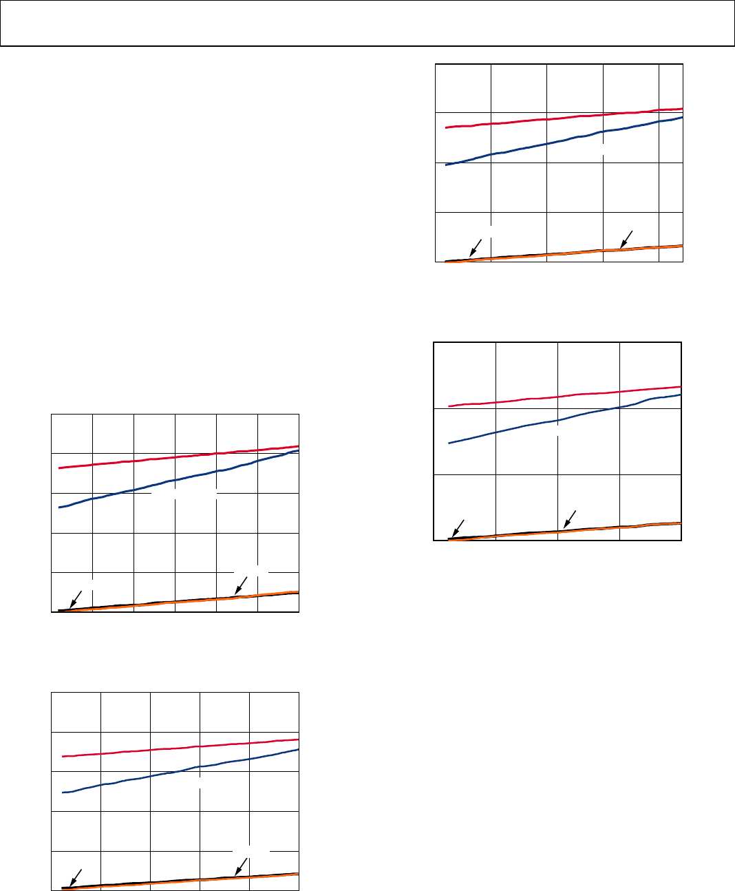
Figure 63. AD9640-150 Power and Current vs. Clock Frequency
0 125
1.25
0.75
1.0
0
06547-075
ENCODE FREQUENCY (MHz)
TOTAL POWER (W)
SUPPLY CURRENT (A)
0.5
0.25
0.5
0.4
0.3
0.2
0.1
0
25 50 75 100
I
AVDD
TOTAL POWER
I
DVDD
I
DRVDD
Figure 64. AD9640-125 Power and Current vs. Clock Frequency
0
1
0
ENCODE FREQUENCY (MHz)
TOTAL POWER (W)
0.75
0.25
0.5
25 50 75 100
06547-074
SUPPLY CURRENT (A)
0.4
0.3
0.2
0.1
0
I
AVDD
TOTAL POWER
I
DRVDD
I
DVDD
Figure 65. AD9640-105 Power and Current vs. Clock Frequency
08
0.75
0
06547-073
ENCODE FREQUENCY (MHz)
TOTAL POWER (W)
SUPPLY CURRENT (A)
0
0.5
0.25
0.3
0.2
0.1
0
20 40 60
I
AVDD
TOTAL POWER
I
DRVDD
I
DVDD
Figure 66. AD9640-80 Power and Current vs. Clock Frequency
By asserting PDWN (either through the SPI port or by asserting
the PDWN pin high), the AD9640 is placed in power-down
mode. In this state, the ADC typically dissipates 2.5 mW.
During power-down, the output drivers are placed in a high
impedance state. Asserting the PDWN pin low returns the
AD9640 to its normal operational mode. Note that PDWN is
referenced to the digital supplies (DRVDD) and should not
exceed that supply voltage.
Low power dissipation in power-down mode is achieved by
shutting down the reference, reference buffer, biasing networks,
and clock. Internal capacitors are discharged when entering power-
down mode and then must be recharged when returning to normal
operation. As a result, wake-up time is related to the time spent
in power-down mode, and shorter power-down cycles result in
proportionally shorter wake-up times.
When using the SPI port interface, the user can place the ADC
in power-down mode or standby mode. Standby mode allows
the user to keep the internal reference circuitry powered when
faster wake-up times are required. See the Memory Map Register
Description section for more details.