
Datasheet


Table Of Contents
- FEATURES
- APPLICATIONS
- FUNCTIONAL BLOCK DIAGRAM
- PRODUCT HIGHLIGHTS
- TABLE OF CONTENTS
- REVISION HISTORY
- GENERAL DESCRIPTION
- SPECIFICATIONS
- ADC DC SPECIFICATIONS—AD9640ABCPZ-80, AD9640BCPZ80, AD9640ABCPZ-105, AND AD9640BCPZ-105
- ADC DC SPECIFICATIONS—AD9640ABCPZ-125, AD9640BCPZ125, AD9640ABCPZ-150, AND AD9640BCPZ150
- ADC AC SPECIFICATIONS—AD9640ABCPZ-80, AD9640BCPZ80, AD9640ABCPZ-105, AND AD9640BCPZ-105
- ADC AC SPECIFICATIONS—AD9640ABCPZ-125, AD9640BCPZ125, AD9640ABCPZ-150, AND AD9640BCPZ 150
- DIGITAL SPECIFICATIONS
- SWITCHING SPECIFICATIONS—AD9640ABCPZ-80, AD9640BCPZ-80, AD9640ABCPZ-105, AND AD9640BCPZ105
- SWITCHING SPECIFICATIONS—AD9640ABCPZ-125, AD9640BCPZ-125, AD9640ABCPZ-150, AND AD9640BCPZ150
- TIMING SPECIFICATIONS
- ABSOLUTE MAXIMUM RATINGS
- PIN CONFIGURATIONS AND FUNCTION DESCRIPTIONS
- EQUIVALENT CIRCUITS
- TYPICAL PERFORMANCE CHARACTERISTICS
- THEORY OF OPERATION
- ADC OVERRANGE AND GAIN CONTROL
- SIGNAL MONITOR
- BUILT-IN SELF-TEST (BIST) AND OUTPUT TEST
- CHANNEL/CHIP SYNCHRONIZATION
- SERIAL PORT INTERFACE (SPI)
- MEMORY MAP
- READING THE MEMORY MAP TABLE
- EXTERNAL MEMORY MAP
- MEMORY MAP REGISTER DESCRIPTION
- Sync Control (Register 0x100)
- Fast Detect Control (Register 0x104)
- Fine Upper Threshold (Register 0x106 and Register 0x107)
- Fine Lower Threshold (Register 0x108 and Register 0x109)
- Signal Monitor DC Correction Control (Register 0x10C)
- Signal Monitor DC Value Channel A (Register 0x10D and Register 0x10E)
- Signal Monitor DC Value Channel B (Register 0x10F and Register 0x110)
- Signal Monitor SPORT Control (Register 0x111)
- Signal Monitor Control (Register 0x112)
- Signal Monitor Period (Register 0x113 to Register 0x115)
- Signal Monitor Result Channel A (Register 0x116 to Register 0x118)
- Signal Monitor Result Channel B (Register 0x119 to Register 0x11B)
- APPLICATIONS INFORMATION
- OUTLINE DIMENSIONS
AD9640
Rev. B | Page 34 of 52
dBFS = 20 log(Threshold Magnitude/2
13
) similarly, corresponds to the fine lower threshold bits, except
that it is asserted only if the input magnitude is less than the
value programmed in the fine lower threshold register after the
dwell time elapses. The dwell time is set by the 16-bit dwell time
value located at Address 0x10A and Address 0x10B and is set in
units of ADC input clock cycles ranging from 1 to 65,535. The
fine lower threshold register is a 13-bit register that is compared
with the magnitude at the output of the ADC. This comparison
is subject to the ADC clock latency but allows a finer, more
accurate comparison. The fine upper threshold magnitude is
defined by the following equation:
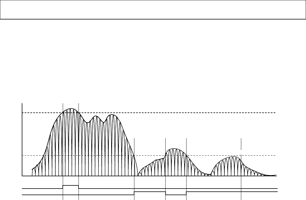
The decrement gain output works from the ADC fast detect
output pins, providing a fast indication of potential overrange
conditions. The increment gain uses the comparison at the
output of the ADC, requiring the input magnitude to remain
below an accurate, programmable level for a predefined period
before signaling external circuitry to increase the gain.
The operation of the increment gain output and the decrement
gain output is shown in Figure 67.
0
6547-097
F_UT
F_LT
FINE UPPER THRESHOLD
FINE LOWER THRESHOLD
Figure 67. Threshold Settings for F_UT and F_LT