
Datasheet


Table Of Contents
- FEATURES
- APPLICATIONS
- FUNCTIONAL BLOCK DIAGRAM
- PRODUCT HIGHLIGHTS
- TABLE OF CONTENTS
- REVISION HISTORY
- GENERAL DESCRIPTION
- SPECIFICATIONS
- ADC DC SPECIFICATIONS—AD9640ABCPZ-80, AD9640BCPZ80, AD9640ABCPZ-105, AND AD9640BCPZ-105
- ADC DC SPECIFICATIONS—AD9640ABCPZ-125, AD9640BCPZ125, AD9640ABCPZ-150, AND AD9640BCPZ150
- ADC AC SPECIFICATIONS—AD9640ABCPZ-80, AD9640BCPZ80, AD9640ABCPZ-105, AND AD9640BCPZ-105
- ADC AC SPECIFICATIONS—AD9640ABCPZ-125, AD9640BCPZ125, AD9640ABCPZ-150, AND AD9640BCPZ 150
- DIGITAL SPECIFICATIONS
- SWITCHING SPECIFICATIONS—AD9640ABCPZ-80, AD9640BCPZ-80, AD9640ABCPZ-105, AND AD9640BCPZ105
- SWITCHING SPECIFICATIONS—AD9640ABCPZ-125, AD9640BCPZ-125, AD9640ABCPZ-150, AND AD9640BCPZ150
- TIMING SPECIFICATIONS
- ABSOLUTE MAXIMUM RATINGS
- PIN CONFIGURATIONS AND FUNCTION DESCRIPTIONS
- EQUIVALENT CIRCUITS
- TYPICAL PERFORMANCE CHARACTERISTICS
- THEORY OF OPERATION
- ADC OVERRANGE AND GAIN CONTROL
- SIGNAL MONITOR
- BUILT-IN SELF-TEST (BIST) AND OUTPUT TEST
- CHANNEL/CHIP SYNCHRONIZATION
- SERIAL PORT INTERFACE (SPI)
- MEMORY MAP
- READING THE MEMORY MAP TABLE
- EXTERNAL MEMORY MAP
- MEMORY MAP REGISTER DESCRIPTION
- Sync Control (Register 0x100)
- Fast Detect Control (Register 0x104)
- Fine Upper Threshold (Register 0x106 and Register 0x107)
- Fine Lower Threshold (Register 0x108 and Register 0x109)
- Signal Monitor DC Correction Control (Register 0x10C)
- Signal Monitor DC Value Channel A (Register 0x10D and Register 0x10E)
- Signal Monitor DC Value Channel B (Register 0x10F and Register 0x110)
- Signal Monitor SPORT Control (Register 0x111)
- Signal Monitor Control (Register 0x112)
- Signal Monitor Period (Register 0x113 to Register 0x115)
- Signal Monitor Result Channel A (Register 0x116 to Register 0x118)
- Signal Monitor Result Channel B (Register 0x119 to Register 0x11B)
- APPLICATIONS INFORMATION
- OUTLINE DIMENSIONS
AD9640
Rev. B | Page 37 of 52
DC Correction Bandwidth
SIGNAL MONITOR SPORT OUTPUT
The dc correction circuit is a high-pass filter with a programmable
bandwidth (ranging between 0.15 Hz and 1.2 kHz at 125 MSPS).
The bandwidth is controlled by writing Bits[5:2] of the signal
monitor dc correction control register, located at Address 0x10C.
The SPORT is a serial interface with three output pins:
SMI SCLK (SPORT clock), SMI SDFS (SPORT frame sync), and
SMI SDO (SPORT data output). The SPORT is the master and
drives all three SPORT output pins on the chip.
The following equation can be used to compute the bandwidth
value for the dc correction circuit:
SMI SCLK
The data output and frame sync are driven on the positive edge of
the SMI SCLK. The SMI SCLK has three possible baud rates: 1/2,
1/4, or 1/8 the ADC clock rate, based on the SPORT controls. The
SMI SCLK can also be gated off when not sending any data, based
on the SPORT SMI SCLK sleep bit. Using this bit to disable the SMI
SCLK when it is not needed can reduce any coupling errors back
into the signal path, if these prove to be a problem in the system.
Doing so, however, has the disadvantage of spreading the frequency
content of the clock. If desired, the SMI SCLK can be left running
to ease frequency planning.
π×
×=
−−
2
2__
14
CLK
k
f
BWCorrDC
where:
k is the 4 bit value programmed in Register 0x10C, Bits[5:2]
(values between 0 and 13 are valid for k; programming 14 or
15 provides the same result as programming 13).
f
CLK
is the ADC sample rate in hertz (Hz).
DC Correction Readback
The current dc correction value can be read back in Register 0x10D
and Register 0x10E for Channel A and in Register 0x10F and
Register 0x110 for Channel B. The dc correction value is a 14-bit
value that can span the entire input range of the ADC.
SMI SDFS
The SMI SDFS is the serial data frame sync, and it defines the
start of a frame. One SPORT frame includes data from both
datapaths. The data from Datapath A is sent just after the frame
sync, followed by data from Datapath B.
DC Correction Freeze
Setting Bit 6 of Register 0x10C freezes the dc correction at its
current state and continues to use the last updated value as the
dc correction value. Clearing this bit restarts dc correction and
adds the currently calculated value to the data.
SMI SDO
The SMI SDO is the serial data output of the block. The data
is sent MSB first on the next positive edge after the SMI SDFS.
Each data output block includes one or more rms/ms magnitude,
peak level, and threshold crossing values from each datapath in
the stated order. If enabled, the data is sent, rms first, followed by
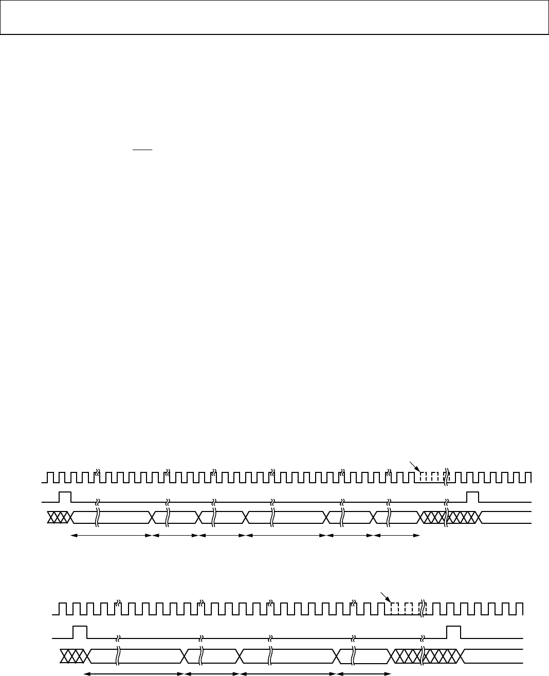
peak and threshold, as shown in Figure 71.
DC Correction Enable Bits
Setting Bit 0 of Register 0x10C enables dc correction for use in
the signal monitor calculations. The calculated dc correction
value can be added to the output data signal path by setting Bit 1
of Register 0x10C.
20 CYCLES 16 CYCLES16 CYCLES 20 CYCLES 16 CYCLES 16 CYCLES
SMI SDFS
MSB MSB
RMS/MS CH A
PK CH A PK CH B
THR CH B
RMS/MS CH B
RMS/MS CH A
LSB
LSB
THR CH A
SMI SDO
S
MI SCLK
GATED, BASED ON CONTROL
06547-094
Figure 71. Signal Monitor SPORT Output Timing (RMS/MS, Peak, and Threshold Enabled)
20 CYCLES 16 CYCLES 20 CYCLES 16 CYCLES
SMI SCLK
SMI SDFS
SMI SDO
MSB MSBRMS/MS CH A RMS/MS CH ALSB THR CH A RMS/MS CH B LSB THR CH B
GATED, BASED ON CONTROL
06547-095
Figure 72. Signal Monitor SPORT Output Timing (RMS/MS and Threshold Enabled)