
Datasheet


Table Of Contents
- FEATURES
- APPLICATIONS
- FUNCTIONAL BLOCK DIAGRAM
- PRODUCT HIGHLIGHTS
- TABLE OF CONTENTS
- REVISION HISTORY
- GENERAL DESCRIPTION
- SPECIFICATIONS
- ADC DC SPECIFICATIONS—AD9640ABCPZ-80, AD9640BCPZ80, AD9640ABCPZ-105, AND AD9640BCPZ-105
- ADC DC SPECIFICATIONS—AD9640ABCPZ-125, AD9640BCPZ125, AD9640ABCPZ-150, AND AD9640BCPZ150
- ADC AC SPECIFICATIONS—AD9640ABCPZ-80, AD9640BCPZ80, AD9640ABCPZ-105, AND AD9640BCPZ-105
- ADC AC SPECIFICATIONS—AD9640ABCPZ-125, AD9640BCPZ125, AD9640ABCPZ-150, AND AD9640BCPZ 150
- DIGITAL SPECIFICATIONS
- SWITCHING SPECIFICATIONS—AD9640ABCPZ-80, AD9640BCPZ-80, AD9640ABCPZ-105, AND AD9640BCPZ105
- SWITCHING SPECIFICATIONS—AD9640ABCPZ-125, AD9640BCPZ-125, AD9640ABCPZ-150, AND AD9640BCPZ150
- TIMING SPECIFICATIONS
- ABSOLUTE MAXIMUM RATINGS
- PIN CONFIGURATIONS AND FUNCTION DESCRIPTIONS
- EQUIVALENT CIRCUITS
- TYPICAL PERFORMANCE CHARACTERISTICS
- THEORY OF OPERATION
- ADC OVERRANGE AND GAIN CONTROL
- SIGNAL MONITOR
- BUILT-IN SELF-TEST (BIST) AND OUTPUT TEST
- CHANNEL/CHIP SYNCHRONIZATION
- SERIAL PORT INTERFACE (SPI)
- MEMORY MAP
- READING THE MEMORY MAP TABLE
- EXTERNAL MEMORY MAP
- MEMORY MAP REGISTER DESCRIPTION
- Sync Control (Register 0x100)
- Fast Detect Control (Register 0x104)
- Fine Upper Threshold (Register 0x106 and Register 0x107)
- Fine Lower Threshold (Register 0x108 and Register 0x109)
- Signal Monitor DC Correction Control (Register 0x10C)
- Signal Monitor DC Value Channel A (Register 0x10D and Register 0x10E)
- Signal Monitor DC Value Channel B (Register 0x10F and Register 0x110)
- Signal Monitor SPORT Control (Register 0x111)
- Signal Monitor Control (Register 0x112)
- Signal Monitor Period (Register 0x113 to Register 0x115)
- Signal Monitor Result Channel A (Register 0x116 to Register 0x118)
- Signal Monitor Result Channel B (Register 0x119 to Register 0x11B)
- APPLICATIONS INFORMATION
- OUTLINE DIMENSIONS
AD9640
Rev. B | Page 41 of 52
CONFIGURATION WITHOUT THE SPI
In applications that do not interface to the SPI control registers,
the SDIO/DCS pin, the SCLK/DFS pin, the SMI SDO/OEB pin,
and the SMI SCLK/PDWN pin serve as standalone, CMOS-
compatible control pins. When the device is powered up, it is
assumed that the user intends to use the pins as static control
lines for the duty cycle stabilizer, output data format, output
enable, and power-down feature control. In this mode, the CSB
chip select should be connected to AVDD, which disables the
serial port interface.
Table 23. Mode Selection
Pin
External
Voltage Configuration
SDIO/DCS AVDD (default) Duty cycle stabilizer enabled.
AGND Duty cycle stabilizer disabled.
SCLK/DFS AVDD Twos complement enabled.
AGND (default) Offset binary enabled.
SMI SDO/OEB AVDD Outputs in high impedance.
AGND (default) Outputs enabled.
SMI SCLK/PDWN AVDD
Chip in power-down or
standby.
AGND (default) Normal operation.
SPI ACCESSIBLE FEATURES
A brief description of general features accessible via the SPI
follows. These features are described in detail in the AN-877
Application Note, Interfacing to High Speed ADCs via SPI. The
AD9640 part-specific features are described in detail following
Table 25, the external memory map register table.
Table 24. Features Accessible Using the SPI
Feature Name Description
Modes
Allows user to set either power-down mode or
standby mode.
Clock Allows user to access the DCS via the SPI.
Offset
Allows user to digitally adjust the converter
offset.
Test I/O
Allows user to set test modes to have known
data on output bits.
Output Mode Allows user to set up outputs.
Output Phase Allows user to set the output clock polarity.
Output Delay Allows user to vary the DCO delay.
VREF Allows user to set the reference voltage.
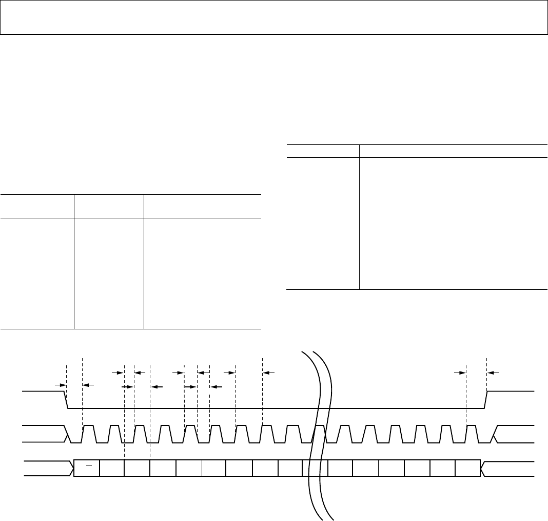
DON’T CARE
DON’T CAREDON’T CARE
DON’T CARE
SDIO
SCLK
CSB
t
S
t
DH
t
CLK
t
DS
t
H
R/W W1 W0 A12 A11 A10 A9 A8 A7
D5 D4 D3 D2 D1 D0
06547-049
t
LOW
t
HIGH
Figure 73. Serial Port Interface Timing Diagram