
Inc. Recording Equipment User Manual
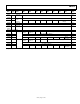
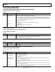
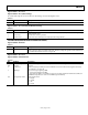
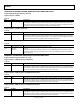
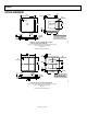

Table Of Contents
- Features
- Applications
- General Description
- Basic Block Diagram
- Revision History
- Specifications
- Absolute Maximum Ratings
- Pin Configuration and Function Descriptions
- Typical Performance Characteristics
- Input/Output Termination Recommendations
- Theory of Operation
- Thermal Performance
- Power-Up
- Power Supply Partitioning
- Serial Control Port
- I/O Register Map
- I/O Register Descriptions
- Serial Port Configuration (Register 0x0000 to Register 0x0005)
- Power-Down and Reset (Register 0x0010 to Register 0x0013)
- System Clock (Register 0x0020 to Register 0x0022)
- CMOS Output Divider (S-Divider) (Register 0x0100 to Register 0x0106)
- Frequency Tuning Word (Register 0x01A0 to Register 0x01AD)
- Register 0x01A0 to Register 0x01A5—Reserved
- Register 0x01A6—FTW0 (Frequency Tuning Word)
- Register 0x01A7—FTW0 (Frequency Tuning Word) (Continued)
- Register 0x01A8—FTW0 (Frequency Tuning Word) (Continued)
- Register 0x01A9—FTW0 (Frequency Tuning Word) (Continued)
- Register 0x01AA—FTW0 (Frequency Tuning Word) (Continued)
- Register 0x01AB—FTW0 (Frequency Tuning Word) (Continued)
- Register 0x01AC—Phase
- Register 0x01AD—Phase (Continued)
- Doubler and Output Drivers (Register 0x0200 to Register 0x0201)
- Calibration (User-Accessible Trim) (Register 0x0400 to Register 0x0410)
- Harmonic Spur Reduction (Register 0x0500 to Register 0x0509)
- Outline Dimensions

AD9912
Rev. D | Page 35 of 40
Register 0x01A9—FTW0 (Frequency Tuning Word) (Continued)
Table 27.
Bits Bit Name Description
[31:24] FTW0 These registers contain the FTW (frequency tuning word) for the DDS. The FTW determines the ratio
of the AD9912 output frequency to its DAC system clock. Register 0x01A6 is the least significant
byte of the FTW. Note that the power-up default is defined by start-up Pin S1 to Pin S4. Updates to
the FTW results in an instantaneous frequency jump but no phase discontinuity.
Register 0x01AA—FTW0 (Frequency Tuning Word) (Continued)
Table 28.
Bits Bit Name Description
[39:32] FTW0 These registers contain the FTW (frequency tuning word) for the DDS. The FTW determines the ratio
of the AD9912 output frequency to its DAC system clock. Register 0x01A6 is the least significant
byte of the FTW. Note that the power-up default is defined by start-up Pin S1 to Pin S4. Updates to
the FTW results in an instantaneous frequency jump but no phase discontinuity.
Register 0x01AB—FTW0 (Frequency Tuning Word) (Continued)
Table 29.
Bits Bit Name Description
[47:40] FTW0 These registers contain the FTW (frequency tuning word) for the DDS. The FTW determines the ratio
of the AD9912 output frequency to its DAC system clock. Register 0x01A6 is the least significant
byte of the FTW. Note that the power-up default is defined by start-up Pin S1 to Pin S4. Updates to
the FTW results in an instantaneous frequency jump but no phase discontinuity.
Register 0x01AC—Phase
Table 30.
Bits Bit Name Description
[7:0] DDS phase word Allows the user to vary the phase of the DDS output. See the Direct Digital Synthesizer section.
Register 0x01AC is the least significant byte of the phase offset word (POW). Note that a momentary
phase discontinuity may occur as the phase passes through 45° intervals.
Register 0x01AD—Phase (Continued)
Table 31.
Bits Bit Name Description
[13:8] DDS phase word Allows the user to vary the phase of the DDS output. See the Direct Digital Synthesizer section.
Register 0x01AC is the least significant byte of the phase offset word (POW). Note that a momentary
phase discontinuity may occur as the phase passes through 45° intervals.