
Datasheet


ADATE207
Rev. 0 | Page 12 of 36
THEORY OF OPERATION
WAVEFORM MEMORY
Pattern data is used to address the waveform memory and is
eight bits wide per channel, supporting 256 unique waveforms.
The data width of the waveform memory is 26 bits wide per
event or 104 bits wide per pin. The waveform memory data bits
are partitioned into two fields, a 22-bit wide delay field, and a
4-bit event code field. The waveform memory is dual port
allowing CPU access during pattern bursting.
Pattern data is used as a pointer to one of the defined 256
waveforms, and can be partitioned into vector data and a time
set pointer. Using three bits of vector data for the pin state, the
other five bits can be used as 32 possible time sets. Supporting
dual I/O per cycle, two sets of 3-bit vector data can be used in
combination with two bits of a time set pointer providing four
possible time sets. A straightforward trade off in time sets vs.
device vectors per tester cycle is possible.
Pattern data is qualified with the input signal PAT_DATA_VALID.
When asserted, the pattern data is evaluated. When not asserted,
events and timing edges are disabled and the input pattern data
is ignored.
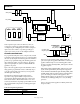
EVENT GENERATORS
Each channel has four programmable event generators. Each
event generator inputs a delay, an event code from the waveform
memory, and an 8-bit INPUT_DELAY. The waveform delay and
the 8-bit INPUT_DELAY combine to produce programmable
delays from T0 cycle starts. Each programmable delay can span
up to 4 T0 periods and up to 163 μs with a nominal delay reso-
lution of 39.06 ps. There are 16 possible events. These events are
compatible with STIL waveform events, as shown in
Table 8, to
create all of the conventional drive and compare formats.
There is a programmable pipeline delay with 2.5 ns resolution
between the drive events and the compare events allowing for
round trip delay (RTD) compensation.
DELAY GENERATION
Each of the four events per channel has an independent delay
generator (D0, D1, D2, and D3). Each delay generator triggers
from a period start using either T0 or C0 periods. A delay value
is the sum of three values: the user programmed delay that is
programmed in waveform memory, a calibration delay indexed
by the selected event, and a global INPUT_DELAY signal that is
used across all channels. These delays are summed and triggered
from the selected period start. The delays are generated using
counts of 2.5 ns plus a 6-bit analog vernier delay. The analog
vernier delay is expressed as a binary fractional value of 2.5 ns.
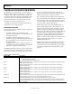
Table 8. STIL-Compatible Events
Code Action Description
N No action Default.
0 Drive low Sets driver to low state.
1 Drive high Sets driver to high state.
Z Force off
Disables the driver and enable
the load.
U Force up
Force Logic high. Enables the
driver and disables the load.
D Force down
Force Logic low. Enables the
driver and disables the load.
P Force prior Enable the driver.
L Compare low Edge compare low.
H Compare high Edge compare high.
X
Compare
unknown
Don’t care. Can be used to close
window compare.
T Compare off Edge compare midband.
V Compare valid Edge compare valid logic level.
l
Compare low
window
Start window compare against
Logic low.
h
Compare high
window
Start window compare against
Logic high.
t
Compare off
window
Start window compare against
midband.
v
Compare valid
window
Start window compare for valid
logic level.
The delay generator uses a value expressed as the binary value
bbbbbbbbbbbbbbbb.vvvvvv where there are 16 bits (b) left of
the binary point and 6 bits (v) right of the binary point. The
b bits represent an integer number of counts of 2.5 ns and the
v bits represent a fractional value of 2.5 ns with a resolution of
2.5 ns/64 or 39.06 ps.
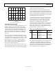
VERNIER RESOLUTION
The analog vernier delays are implemented using a modulo 60
algorithm and dividing 2.5 ns into 60 even parts. Because the
delays are expressed using a binary representation, an internal
mapping algorithm generates the delays. Ignoring analog timing
errors, the actual delay produced for the six bits of vernier value
(vvvvvv) is expressed as
Delay = (2.5 ns/60) × INT (.5 + (vvvvvv × 60/64))
This mapping results in an inherent discontinuity in the
linearity curve.
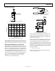
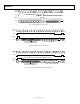
Figure 7 shows the linearity of a typical vernier. On certain
delay codes, the vernier exhibits non-monotonicity. To obtain a
monotonic delay curve, these code jumps should be ignored by
the user.