
Datasheet


ADATE207
Rev. 0 | Page 14 of 36
T0 M C
M M
T0 M
INPUT_DELAY
C
44 11
C
11
PROGRAMMABLE
RTD DELAY [0:31]
C
1
C
DUT
C
FIFO
2
T0
PROGRAMMABLE
T0 DELAY [0:30]
T0
T0
3
PAT_PATDAT
A
FAIL
DUTDATA
LEGEND
1
RTD COMPENSATION
CLK400
PIPELINE
REGISTER
MCLK
PIPELINE
REGISTER
T0
PIPELINE
REGISTER
05557-002
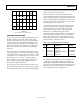
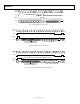
Figure 8. Pipeline Diagram
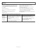
Dual comparator inputs of the even channels (0 and 2) are
routed to the compare logic of adjacent channels to provide
×2 multiplexing. In ×2 multiplexing, Pin 0 and Pin 2 comparator
inputs route to Pin 1 and Pin 3, respectively, providing up to
eight compare events per cycle on the multiplexed channels.
PIPELINE CONSIDERATIONS
For proper functionality, drive actions, compare events, and fail
accumulation mask requirements need to be coordinated within
the device by adjusting the internal delay paths. The ADATE207
provides two programmable delay paths, the RTD pipeline and
the T0 alignment pipeline, as shown in
Figure 8. The pattern
input and output signals are synchronous with the MCLK and
pipelined on T0 periods.
Figure 8 shows the pipeline diagram of the ADATE207. The T0
delay pipeline is programmable. It must be sufficiently deep to
cover the round trip delay compensation, yet no deeper than
the FIFO depth of the fail logic.
The minimum T0 alignment pipeline depth needed is
dependent on the programmed RTD compensation. The
programmed T0 alignment pipeline depth must conform to the
values listed in
Tabl e 10. The maximum number of 30 can be
used in any circumstance. Depending upon the MCLK rate and
the programmed RTD compensation, a smaller pipeline depth
can be used.
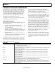
Table 10. T0 Pipeline Requirements
T0 Alignment Pipelines
Minimum Maximum
10.5 + RTD/4 30
MCLK
QD
CE
T0 PIPELINE
PER_EARLY_T0EN
PER_EARLY_C0EN
PAT_PATDATA_x[7:0]
PAT_DATA_VALID
PAT_MASK[3:0]
INPUT_DELAY[7:0]
05557-020
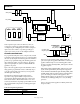
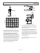
Figure 9. PER_EARLY_T0EN Pipelining
Figure 9 shows the pipelining of PER_EARLY_T0EN (the
period start signal). It is pipelined with MCLK to control the T0
pipelines within the chip. It uses two MCLK pipelines within
the chip to distribute the PER_EARLY_T0EN signal to all of the
T0 pipeline registers.
PER_EARLY_T0EN and PER_EARLY_C0EN, the period start
signals, and the global INPUT_DELAY signals are pipelined
into the ADATE207 with different depths. The PER_EARLY_T0EN
and PER_EARLY_C0EN are pipelined with two MCLK pipelines
prior to the enable pins of the T0 clocked pipelines. The
INPUT_DELAY signals are not pipelined on T0 clock pipelines,
but have only two MCLK pipelines prior to use by the timing
generators.
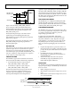
Figure 10 shows the relative pipelines for INPUT_DELAY and
the period enables.