
Datasheet

ADATE207
Rev. 0 | Page 27 of 36
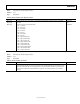
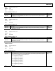
Name: Waveform D2 Vernier Delay and Action
Address: 0x0A
Type: Read/Write
Table 24. Waveform D2 Vernier Delay and Action
Position Description Reset State
Bits[15:10]
D2 Vernier Delay: The vernier delay is represented in binary by the equation,
vvvvvv × (2.5 ns/64)
Undefined
Bits[09:04] Not Used. 0x00
Bits[03:00] D2 Action. A binary encoded data field. Undefined
0x0 = no action.
0x1 = drive low.
0x2 = drive high.
0x3 = force off.
0x4 = force on.
0x5 = force down.
0x6 = force up.
0x7 = edge compare low.
0x8 = edge compare high.
0x9 = edge compare off.
0xA = edge compare valid.
0xB = open window low.
0xC = open window high.
0xD = open window high-Z.
0xE = open window valid.
0xF = compare unknown.
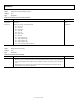
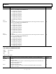
Name: Waveform D2 C ourse De lay
Address: 0x0B
Type: Read/Write
Table 25. Waveform D2 Course Delay
Position Description Reset State
Bits[15:00] D2 Course Delay. Number of 2.5 ns clock periods to count. Undefined
When this count is completed, the vernier delay (defined by the D2 vernier value programmed
into the waveform D2 vernier delay and action register) is added to the D2 course delay to
place an edge in time
Waveform D2 vernier delay and action must be written immediately before this register for the
waveform memory to be correctly written.