Single-Phase Energy Measurement IC with 8052 MCU, RTC, and LCD Driver ADE5166/ADE5169/ADE5566/ADE5569 Data Sheet GENERAL FEATURES MICROPROCESSOR FEATURES Wide supply voltage operation: 2.4 V to 3.7 V Internal bipolar switch between regulated and battery inputs Ultralow power operation with power saving modes (PSM) Full operation: 4.4 mA to 1.6 mA (PLL clock dependent) Battery mode: 3.3 mA to 400 µA (PLL clock dependent) Sleep mode Real-time clock (RTC) mode: 1.
ADE5166/ADE5169/ADE5566/ADE5569 Data Sheet TABLE OF CONTENTS General Features ............................................................................... 1 Fault Detection (ADE5166/ADE5169 Only) .......................... 52 Energy Measurement Features........................................................ 1 Microprocessor Features.................................................................. 1 di/dt Current Sensor and Digital Integrator (ADE5169/ADE5569 Only) .................................
Data Sheet ADE5166/ADE5169/ADE5566/ADE5569 Writing to the Watchdog Timer SFR (WDCON, Address 0xC0).............................................................................................99 RTC Crystal Compensation ....................................................128 UART Serial Interface ...................................................................129 Watchdog Timer Interrupt.........................................................99 UART SFRs .............................................
ADE5166/ADE5169/ADE5566/ADE5569 Data Sheet REVISION HISTORY 4/12—Rev. C to Rev. D Changes to Table 1 ............................................................................. 1 Moved Revision History ................................................................... 4 Added 32 kB Flash Option Section ................................................. 5 Changes to Vrms Measurement Bandwidth Parameter, Table 2 ... 7 Changes to Table 17 ....................................................................
Data Sheet ADE5166/ADE5169/ADE5566/ADE5569 GENERAL DESCRIPTION The ADE5166/ADE5169 include a 104-segment LCD driver and the ADE5566/ADE5569 include a 108-segment LCD driver, each with the capability to store up to four LCD screens in memory. This driver generates voltages capable of driving LCDs up to 5 V. The ADE5166/ADE5169/ADE5566/ADE55691 integrate the Analog Devices, Inc.
P1.5/FP22 P1.6/FP21 6 7 8 9 10 P1.7/FP20 P1.
Data Sheet ADE5166/ADE5169/ADE5566/ADE5569 SPECIFICATIONS VDD = 3.3 V ± 5%, AGND = DGND = 0 V, on-chip reference XTALx = 32.768 kHz, TMIN to TMAX = −40°C to +85°C, unless otherwise noted. ENERGY METERING Table 2. Parameter MEASUREMENT ACCURACY 1 Phase Error Between Channels PF = 0.8 Capacitive PF = 0.
ADE5166/ADE5169/ADE5566/ADE5569 Data Sheet ANALOG PERIPHERALS Table 3. Parameter INTERNAL ADCs (BATTERY, TEMPERATURE, VDCIN) Power Supply Operating Range No Missing Codes 1 Conversion Delay 2 ADC Gain VDCIN Measurement VBAT Measurement Temperature Measurement ADC Offset VDCIN Measurement at 3 V VBAT Measurement at 3.
Data Sheet Parameter LCD, RESISTOR LADDER ACTIVE Leakage Current V1 Segment Line Voltage V2 Segment Line Voltage V3 Segment Line Voltage ON-CHIP REFERENCE Reference Error Power Supply Rejection Temperature Coefficient1 1 2 ADE5166/ADE5169/ADE5566/ADE5569 Min Typ Max Unit Test Conditions/Comments LCDVA LCDVB LCDVC nA V V V 1/2 and 1/3 bias modes, no load Current on segment line = −2 µA Current on segment line = −2 µA Current on segment line = −2 µA Nominal 1.2035 V TA = 25°C, fCORE = 1.
ADE5166/ADE5169/ADE5566/ADE5569 Parameter POWER SUPPLY INPUTS VDD VBAT INTERNAL POWER SUPPLY SWITCH (VSWOUT) VBAT to VSWOUT On Resistance VDD to VSWOUT On Resistance VBAT to/from VDD Switching Open Time BCTRL State Change and Switch Delay VSWOUT Output Current Drive POWER SUPPLY OUTPUTS VINTA VINTD VINTA Power Supply Rejection VINTD Power Supply Rejection POWER SUPPLY CURRENTS Current in Normal Mode (PSM0) Current in Battery Mode (PSM1) Current in Sleep Mode (PSM2) Data Sheet Min Typ Max Unit 3.13 2.
Data Sheet ADE5166/ADE5169/ADE5566/ADE5569 TIMING SPECIFICATIONS For timing purposes, a port pin is no longer floating when a 100 mV change from load voltage occurs. A port pin begins to float when a 100 mV change from the loaded VOH/VOL level occurs, as shown in Figure 3. AC inputs during testing were driven at VSWOUT − 0.5 V for Logic 1 and at 0.45 V for Logic 0. Timing measurements were made at VIH minimum for Logic 1 and at VIL maximum for Logic 0, as shown in Figure 3. VLOAD – 0.1V 0.2VSWOUT + 0.
ADE5166/ADE5169/ADE5566/ADE5569 Data Sheet Table 7. SPI Master Mode Timing Parameters (SPICPHA = 1) Parameter tSL tSH tDAV tDSU tDHD tDF tDR tSR tSF Min 2SPIR × tCORE 1 2SPIR × tCORE1 Typ Max 3 × tCORE1 0 tCORE1 19 19 19 19 tCORE depends on the clock divider or the CD bits of the POWCON SFR, Address 0xC5[2:0] (see Table 26); tCORE = 2CD/4.096 MHz. SCLK (SPICPOL = 0) tSH tSL tSR SCLK (SPICPOL = 1) tDAV tDF tSF tDR MOSI BITS[6:1] MSB MISO MSB IN tDSU BITS[6:1] tDHD Figure 5.
Data Sheet ADE5166/ADE5169/ADE5566/ADE5569 Table 8. SPI Master Mode Timing Parameters (SPICPHA = 0) Parameter tSL tSH tDAV tDOSU tDSU tDHD tDF tDR tSR tSF Min 2SPIR × tCORE 1 2SPIR × tCORE1 Typ (SPIR + 1) × tCORE1 (SPIR + 1) × tCORE1 Max 3 × tCORE1 75 0 tCORE1 19 19 19 19 tCORE depends on the clock divider or the CD bits of the POWCON SFR, Address 0xC5[2:0] (see Table 26); tCORE = 2CD/4.096 MHz.
ADE5166/ADE5169/ADE5566/ADE5569 Data Sheet Table 9. SPI Slave Mode Timing Parameters (SPICPHA = 1) Parameter tSS Description SS to SCLK edge Min 145 tSL tSH tDAV tDSU tDHD tDF tDR tSR tSF tSFS SCLK low pulse width SCLK high pulse width Data output valid after SCLK edge Data input setup time before SCLK edge Data input hold time after SCLK edge Data output fall time Data output rise time SCLK rise time SCLK fall time SS high after SCLK edge 6 × tCORE 1 6 × tCORE1 Max 25 0 2 × tCORE1 + 0.
Data Sheet ADE5166/ADE5169/ADE5566/ADE5569 Table 10.
ADE5166/ADE5169/ADE5566/ADE5569 Data Sheet ABSOLUTE MAXIMUM RATINGS TA = 25°C, unless otherwise noted. Table 11. Parameter VDD to DGND VBAT to DGND VDCIN to DGND Input LCD Voltage to AGND, LCDVA, LCDVB, LCDVC1 Analog Input Voltage to AGND, VP, VN, IP/IPA, IPB, and IN Digital Input Voltage to DGND Digital Output Voltage to DGND Operating Temperature Range (Industrial) Storage Temperature Range 64-Lead LQFP, Power Dissipation Lead Temperature (Soldering, 30 sec) 1 Rating −0.3 V to +3.7 V −0.3 V to +3.
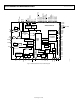
Data Sheet ADE5166/ADE5169/ADE5566/ADE5569 VN VP IPA EA AGND IN RESET IPB VBAT REFIN/OUT VDD VINTA VINTD VSWOUT VDCIN DGND PIN CONFIGURATIONS AND FUNCTION DESCRIPTIONS 64 63 62 61 60 59 58 57 56 55 54 53 52 51 50 49 COM3/FP27 1 COM2/FP28 2 48 INT0 PIN 1 47 XTAL1 46 XTAL2 COM1 3 COM0 4 45 BCTRL/INT1/P0.0 P1.2/FP25/ZX 5 44 SDEN/P2.3/TxD2 P1.3/T2EX/FP24 6 43 P0.2/CF1 P1.4/T2/FP23 7 42 P0.3/CF2 P1.5/FP22 8 ADE5166/ADE5169 P1.6/FP21 9 TOP VIEW (Not to Scale) 41 P0.
ADE5166/ADE5169/ADE5566/ADE5569 Pin No. 42 Mnemonic P0.3/CF2 43 P0.2/CF1 44 SDEN/P2.3/TxD2 45 BCTRL/INT1/P0.0 46 XTAL2 47 XTAL1 48 49, 50 INT0 VP, VN 51 EA 52, 53 IPA, IN 54 55 AGND IPB 56 57 RESET REFIN/OUT 58 VBAT 59 VINTA 60 VDD 61 VSWOUT 62 VINTD 63 64 DGND VDCIN Data Sheet Description General-Purpose Digital I/O Port 0.3/Calibration Frequency Logic Output 2. The CF2 logic output gives instantaneous active, reactive, or apparent power or Irms information.
VP EA VN IN IP FP26 AGND RESET VBAT REFIN/OUT VDD VINTA VINTD VSWOUT VDCIN ADE5166/ADE5169/ADE5566/ADE5569 DGND Data Sheet 64 63 62 61 60 59 58 57 56 55 54 53 52 51 50 49 COM3/FP27 1 COM2/FP28 2 48 INT0 PIN 1 47 XTAL1 46 XTAL2 COM1 3 COM0 4 45 BCTRL/INT1/P0.0 P1.2/FP25/ZX 5 44 SDEN/P2.3/TxD2 P1.3/T2EX/FP24 6 43 P0.2/CF1 P1.4/T2/FP23 7 42 P0.3/CF2 P1.5/FP22 8 ADE5566/ADE5569 P1.6/FP21 9 TOP VIEW (Not to Scale) 41 P0.4/MOSI/SDATA 40 P0.5/MISO/ZX P1.
ADE5166/ADE5169/ADE5566/ADE5569 Pin No. 43 Mnemonic P0.2/CF1 44 SDEN/P2.3/TxD2 45 BCTRL/INT1/P0.0 46 XTAL2 47 XTAL1 48 49, 50 INT0 VP, VN 51 EA 52, 53 IP, IN 54 55 56 57 AGND FP26 RESET REFIN/OUT 58 VBAT 59 VINTA 60 VDD 61 VSWOUT 62 VINTD 63 64 DGND VDCIN Data Sheet Description General-Purpose Digital I/O Port 0.2/Calibration Frequency Logic Output 1. The CF1 logic output gives instantaneous active, reactive, or apparent power or Irms information.
Data Sheet ADE5166/ADE5169/ADE5566/ADE5569 TYPICAL PERFORMANCE CHARACTERISTICS 2.0 2.0 1.5 MID CLASS C GAIN = 1 INTEGRATOR OFF INTERNAL REFERENCE 1.5 1.0 0.5 +25°C; PF = 1 ERROR (% of Reading) 1.0 ERROR (% of Reading) GAIN = 1 INTEGRATOR OFF INTERNAL REFERENCE +85°C; PF = 1 0 –40°C; PF = 1 –0.5 0.5 +25°C; PF = 0 +85°C; PF = 0 –40°C; PF = 0.866 0 –40°C; PF = 0 +25°C; PF = 0.866 –0.5 –1.0 –1.0 –1.5 –1.5 1 10 100 CURRENT CHANNEL (% of Full Scale) Figure 11.
ADE5166/ADE5169/ADE5566/ADE5569 Data Sheet 0.5 1.5 GAIN = 1 INTEGRATOR OFF INTERNAL REFERENCE 0.4 1.0 0.2 ERROR (% of Reading) ERROR (% of Reading) 0.3 VRMS; 3.3V IRMS; 3.13V 0.1 VRMS; 3.43V IRMS; 3.3V 0 VRMS; 3.13V –0.1 IRMS; 3.43V –0.2 GAIN = 8 INTEGRATOR OFF INTERNAL REFERENCE –0.3 MID CLASS C 0.5 PF = +1 0 PF = +0.5 PF = –0.5 –0.5 MID CLASS C –1.0 1 10 100 CURRENT CHANNEL (% of Full Scale) –1.5 0.1 07411-132 –0.5 0.1 Figure 17.
Data Sheet ADE5166/ADE5169/ADE5566/ADE5569 2.0 1.5 1.0 MID CLASS C GAIN = 16 INTEGRATOR OFF INTERNAL REFERENCE 0.8 GAIN = 16 INTEGRATOR OFF INTERNAL REFERENCE 0.6 +85°C; PF = 0.866 0.5 ERROR (% of Reading) ERROR (% of Reading) 1.0 +85°C; PF = 1 +25°C; PF = 1 0 –40°C; PF = 1 –0.5 +85°C; PF = 0 0.4 –40°C; PF = 0.866 –40°C; PF = 0 0.2 0 +25°C; PF = 0.866 +25°C; PF = 0 –0.2 –0.4 –1.0 –0.6 –1.5 1 10 100 CURRENT CHANNEL (% of Full Scale) –1.0 0.1 07411-138 –2.0 0.1 Figure 23.
ADE5166/ADE5169/ADE5566/ADE5569 Data Sheet 2.0 1.5 1.0 –40°C; PF = 1 0.5 +85°C; PF = 1 +85°C; PF = 0.5 0 –40°C; PF = 0.5 –0.5 +25°C; PF = 1 +25°C; PF = 0.5 –1.0 0.5 +85°C; PF = 1 0 –0.5 –40°C; PF = 0.5 –40°C; PF = 1 +25°C; PF = 0.5 +25°C; PF = 1 –1.5 MID CLASS C 1 10 MID CLASS C 100 CURRENT CHANNEL (% of Full Scale) –2.0 0.1 07411-144 –2.0 0.1 Figure 29. Active Energy Error as a Percentage of Reading (Gain = 16) over Power Factor with Internal Reference, Integrator On 0.
Data Sheet ADE5166/ADE5169/ADE5566/ADE5569 TERMINOLOGY Measurement Error The error associated with the energy measurement made by the ADE5166/ADE5169/ADE5566/ADE5569 is defined by the following formula: with the same input signal levels when an ac signal (100 mV rms/ 120 Hz) is introduced onto the supplies. Any error introduced by this ac signal is expressed as a percentage of the reading (see the Measurement Error definition). For the dc PSR measurement, a reading at nominal supplies (3.3 V) is taken.
ADE5166/ADE5169/ADE5566/ADE5569 Data Sheet SPECIAL FUNCTION REGISTER (SFR) MAPPING Table 15.
Data Sheet Mnemonic SBAUDT Address 0x9E SBAUDF 0x9D LCDCONX SPI2CRx SPI2CTx SBUF SCON 0x9C 0x9B 0x9A 0x99 0x98 LCDSEGE LCDCLK LCDCON MDATH 0x97 0x96 0x95 0x94 MDATM 0x93 MDATL 0x92 ADE5166/ADE5169/ADE5566/ADE5569 Description Enhanced serial baud rate control (see Table 142). UART timer fractional divider (see Table 143). LCD Configuration X (see Table 92). SPI/I2C receive buffer (see Table 152). SPI/I2C transmit buffer (see Table 151). Serial port buffer (see Table 141).
ADE5166/ADE5169/ADE5566/ADE5569 Data Sheet POWER MANAGEMENT The ADE5166/ADE5169/ADE5566/ADE5569 have elaborate power management circuitry that manages the regular power supply to battery switchover and power supply failures. The power management functionalities can be accessed directly through the 8052 power management SFRs (see Table 16). Table 16.
Data Sheet ADE5166/ADE5169/ADE5566/ADE5569 Table 18. Power Management Interrupt Flag SFR (IPSMF, Address 0xF8) Bit 7 Bit Address 0xFF Mnemonic FPSR Default 0 6 5 4 3 0xFE 0xFD 0xFC 0xFB FPSM FSAG Reserved FVADC 0 0 0 0 2 0xFA FBAT 0 1 0 0xF9 0xF8 FBSO FVDCIN 0 0 Description Power supply restored interrupt flag. Set when the VDD power supply has been restored. This occurs when the source of VSWOUT changes from VBAT to VDD. PSM interrupt flag.
ADE5166/ADE5169/ADE5566/ADE5569 Data Sheet Table 22. Scratch Pad 1 SFR (SCRATCH1, Address 0xFB) Bit [7:0] Mnemonic SCRATCH1 Default 0 Description Value can be written/read in this register. This value is maintained in all the power saving modes. Table 23. Scratch Pad 2 SFR (SCRATCH2, Address 0xFC) Bit [7:0] Mnemonic SCRATCH2 Default 0 Description Value can be written/read in this register. This value is maintained in all the power saving modes. Table 24.
Data Sheet ADE5166/ADE5169/ADE5566/ADE5569 POWER SUPPLY ARCHITECTURE The ADE5166/ADE5169/ADE5566/ADE5569 have two power supply inputs, VDD and VBAT. They require only a single 3.3 V power supply at VDD for full operation. A battery backup, or secondary power supply, with a maximum of 3.7 V can be connected to the VBAT input. Internally, the ADE5166/ADE5169/ADE5566/ ADE5569 connect VDD or VBAT to VSWOUT, which is used to derive power for the ADE5166/ADE5169/ADE5566/ADE5569 circuitry.
ADE5166/ADE5169/ADE5566/ADE5569 Data Sheet EPSR FPSR ESAG FSAG EVADC FVADC FPSM TRUE? EPSM PENDING PSM INTERRUPT EBAT FBAT EBSO FBSO EVDCIN FVDCIN EPSR RESERVED ESAG RESERVED EVADC EBAT EBSO EVDCIN IPSMF ADDR. 0xF8 FPSR FPSM FSAG RESERVED FVADC FBAT FBSO FVDCIN IEIP2 ADDR. 0xA9 PS2 PTI ES2 PSI EADE ETI EPSM ESI 07411-012 IPSME ADDR. 0xEC NOT INVOLVED IN PSM INTERRUPT SIGNAL CHAIN Figure 33.
Data Sheet ADE5166/ADE5169/ADE5566/ADE5569 SAG Monitor PSM Interrupt The ADE5166/ADE5169/ADE5566/ADE5569 energy measurement DSP monitors the ac voltage input at the VP and VN input pins. The SAGLVL register (Address 0x14) is used to set the threshold for a line voltage SAG event.
ADE5166/ADE5169/ADE5566/ADE5569 Data Sheet VP – VN SAG LEVEL TRIP POINT SAGCYC = 1 VDCIN 1.2V t1 VDD 2.75V t2 VDCIN EVENT (FVDCIN = 1) IF SWITCHOVER ON LOW VDD IS ENABLED, AUTOMATIC BATTERY SWITCHOVER OCCURS. VSWOUT IS CONNECTED TO VBAT . BSO EVENT (FBSO = 1) 07411-014 SAG EVENT (FSAG = 1) Figure 35. Power Supply Management Interrupts and Battery Switchover with Only VDD Enabled for Battery Switchover VP – VN SAG LEVEL TRIP POINT SAGCYC = 1 VDCIN 1.2V t3 t1 VDD 2.
Data Sheet ADE5166/ADE5169/ADE5566/ADE5569 VP − VN SAG LEVEL TRIP POINT SAG EVENT VDCIN EVENT VDCIN VDCIN EVENT 1.2V 30ms 130ms VBAT VDD 2.75V VSWOUT PSM0 BATTERY SWITCH ENABLED ON LOW VDCIN PSM0 PSM1 OR PSM2 VSWOUT PSM0 PSM1 OR PSM2 Figure 37. Power Supply Management Transitions Between Modes Rev.
ADE5166/ADE5169/ADE5566/ADE5569 Data Sheet OPERATING MODES PSM0 (NORMAL MODE) In PSM0 mode, or normal operating mode, VSWOUT is connected to VDD. All of the analog circuitry and digital circuitry powered by VINTD and VINTA are enabled by default. In normal mode, the default clock frequency, fCORE, which is established during a power-on reset or software reset, is 1.024 MHz. PSM1 (BATTERY MODE) In PSM1 mode, or battery mode, VSWOUT is connected to VBAT.
Data Sheet ADE5166/ADE5169/ADE5566/ADE5569 3.3 V PERIPHERALS AND WAKE-UP EVENTS Some of the 3.3 V peripherals are capable of waking the ADE5166/ ADE5169/ADE5566/ADE5569 from PSM2 mode. The events that can cause the ADE5166/ADE5169/ADE5566/ADE5569 to wake up from PSM2 mode are listed in the wake-up event column in Table 29. The interrupt flag associated with these events must be cleared prior to executing instructions that put the ADE5166/ ADE5169/ADE5566/ADE5569 in PSM2 mode after wake-up. Table 29. 3.
ADE5166/ADE5169/ADE5566/ADE5569 Data Sheet TRANSITIONING BETWEEN OPERATING MODES Automatic Switch to VDD (PSM1 to PSM0) The operating mode of the ADE5166/ADE5169/ADE5566/ ADE5569 is determined by the power supply connected to VSWOUT. Therefore, changes in the power supply, such as when VSWOUT switches from VDD to VBAT or when VSWOUT switches to VDD, alter the operating mode. This section describes events that change the operating mode.
Data Sheet ADE5166/ADE5169/ADE5566/ADE5569 ENERGY MEASUREMENT The ADE5166/ADE5169/ADE5566/ADE5569 offer a fixed function, energy measurement, digital processing core that provides all the information needed to measure energy in single-phase energy meters. The part provides two ways to access the energy measurements: direct access through SFRs for time sensitive information and indirect access through address and data SFRs for the majority of energy measurements.
ADE5166/ADE5169/ADE5566/ADE5569 Data Sheet Table 31. Energy Measurement SFRs Address 0x91 0x92 0x93 0x94 0xD1 0xD2 0xD3 0xD4 0xD5 0xD6 0xD9 0xDA 0xDB 0xDC 0xDD 0xDE 0xE2 0xE3 0xE4 0xE5 0xE6 0xE7 IPA R/W R/W R/W R/W R/W R R R R R R R/W R/W R/W R/W R/W R/W R R R R R R Mnemonic MADDPT MDATL MDATM MDATH VRMSL VRMSM VRMSH IRMSL IRMSM IRMSH MIRQENL MIRQENM MIRQENH MIRQSTL MIRQSTM MIRQSTH WAV1L WAV1M WAV1H WAV2L WAV2M WAV2H Description Energy measurement pointer address. Energy measurement pointer data LSB.
Data Sheet IPA ×1, ×2, ×4, ×8, ×16 {GAIN[2:0]} WGAIN[11:0] INTEGRATOR MULTIPLIER PGA1 I ADE5166/ADE5169/ADE5566/ADE5569 dt ADC LPF2 HPF IN CF1NUM[15:0] PHCAL[7:0] WATTOS[15:0] π 2 VARGAIN[11:0] CF1 DFC Ф LPF2 CF1DEN[15:0] IRMSOS[11:0] VAROS[15:0] CF2NUM[15:0] VAGAIN[11:0] LPF2 HPF x2 VARDIV[7:0] VP CF2DEN[15:0] ADC HPF LPF1 |X| LPF3 VADIV[7:0] % % % METERING SFRs Figure 40. ADE5566/ADE5569 Energy Metering Block Diagram Rev.
ADE5166/ADE5169/ADE5566/ADE5569 Data Sheet ENERGY MEASUREMENT REGISTERS Table 32.
Data Sheet Address MADDPT[6:0] 0x29 0x2A 0x2B 0x3B 0x3C 0x3D 0x3E 0x3F 1 2 ADE5166/ADE5169/ADE5566/ADE5569 Mnemonic CF2NUM CF2DEN MODE3 Reserved Reserved CALMODE2 Reserved Reserved R/W R/W R/W R/W Length (Bits) 16 16 8 Signed/ Unsigned U U U R/W 8 U Default 0 0x003F 0 0 0x0300 0 0 0 Description Sets CF2 numerator register. Sets CF2 denominator register. Enables zero-crossing outputs (see Table 39). This register must be set to its default value for proper operation.
ADE5166/ADE5169/ADE5566/ADE5569 Data Sheet Table 35. Waveform Mode Register (WAVMODE, Address 0x0D) Bit [7:5] Mnemonic WAV2SEL Default 000 [4:2] WAV1SEL 000 [1:0] DTRT 00 1 Description Waveform Sample 2 selection for samples mode. WAV2SEL Source 000 Current 001 Voltage 010 Active power multiplier output 011 Reactive power multiplier output 1 100 VA multiplier output 101 Irms LPF output (low 24-bit) 110, 111 Reserved Waveform Sample 1 selection for samples mode.
Data Sheet ADE5166/ADE5169/ADE5566/ADE5569 Table 37. Accumulation Mode Register (ACCMODE, Address 0x0F) Bit 7 Mnemonic ICHANNEL 1 Default 0 6 FAULTSIGN1 0 5 VARSIGN 2 0 4 APSIGN 0 3 2 ABSVARM2 SAVARM2 0 0 1 0 POAM ABSAM 0 0 1 2 Description This bit indicates the current channel used to measure energy in antitampering mode. 0 = Channel A (IPA). 1 = Channel B (IPB). Configuration bit to select the event that triggers a fault interrupt.
ADE5166/ADE5169/ADE5566/ADE5569 Data Sheet Table 40. Calibration Mode Register (CALMODE, Address 0x3D) 1 Bit [7:6] [5:4] Mnemonic Reserved SEL_I_CH Default 00 00 3 2 [1:0] V_CH_SHORT I_CH_SHORT Reserved 0 0 00 1 Description These bits must be kept at 0 for proper operation. These bits define the current channel used for energy measurements.
Data Sheet ADE5166/ADE5169/ADE5566/ADE5569 Table 44. Interrupt Enable 1 SFR (MIRQENL, Address 0xD9) Bit [7:6] 5 4 3 2 1 0 1 2 Interrupt Enable Bit Reserved FAULTSIGN 1 VARSIGN 2 APSIGN VANOLOAD RNOLOAD2 APNOLOAD Description Reserved. When this bit is set to Logic 1, the FAULTSIGN flag set creates a pending ADE interrupt to the 8052 core. When this bit is set to Logic 1, the VARSIGN flag set creates a pending ADE interrupt to the 8052 core.
ADE5166/ADE5169/ADE5566/ADE5569 Data Sheet ANALOG-TO-DIGITAL CONVERSION ADE5169/ADE5566/ADE5569 is 4.096 MHz/5 (819.2 kHz); and the band of interest is 40 Hz to 2 kHz. Oversampling has the effect of spreading the quantization noise (noise due to sampling) over a wider bandwidth. With the noise spread more thinly over a wider bandwidth, the quantization noise in the band of interest is lowered (see Figure 43). Each ADE5166/ADE5169/ADE5566/ADE5569 has two Σ-Δ analog-to-digital converters (ADCs).
Data Sheet ADE5166/ADE5169/ADE5566/ADE5569 Antialiasing Filter Figure 44 also shows an analog LPF (RC) on the input to the modulator. This filter is present to prevent aliasing, an artifact of all sampled systems. Aliasing means that frequency components in the input signal to the ADC that are higher than half the sampling rate of the ADC appear in the sampled signal at a frequency below half the sampling rate. Figure 45 illustrates the effect.
ADE5166/ADE5169/ADE5566/ADE5569 ×1, ×2, ×4 ×8, ×16 {GAIN[2:0]} Data Sheet MODE1[5] WAVEFORM SAMPLE REGISTER DIGITAL INTEGRATOR* IPA PGA1 I CURRENT RMS (I rms) CALCULATION REFERENCE ADC ACTIVE AND REACTIVE POWER CALCULATION dt HPF IN PGA1 HPF IPB V1 CURRENT CHANNEL WAVEFORM DATA RANGE AFTER INTEGRATOR (50Hz) 50Hz ADC 0x342CD0 0.25V, 0.125V, 62.5mV, 31.
Data Sheet ADE5166/ADE5169/ADE5566/ADE5569 Voltage Channel ADC Figure 48 shows the ADC and signal processing chain for the voltage channel. In waveform sampling mode, the ADC outputs a signed, twos complement, 24-bit data-word at a maximum of 25.6 kSPS (MCLK/160). The ADC produces an output code that is approximately between 0x28F5 (+10,485d) and 0xD70B (−10,485d).
ADE5166/ADE5169/ADE5566/ADE5569 Data Sheet FAULT DETECTION (ADE5166/ADE5169 ONLY) Fault with Active Input Greater Than Inactive Input The ADE5166/ADE5169 incorporate a fault detection scheme that warns of fault conditions and allows accurate measurement to continue during a fault event. (This feature is not available in the ADE5566/ADE5569.) The ADE5166/ADE5169 do this by continuously monitoring both current inputs (IPA and IPB).
Data Sheet ADE5166/ADE5169/ADE5566/ADE5569 For calibration, a first measurement should be done on IPA by setting the SEL_I_CH bits (Bits[5:4]) to 0b01 in the CALMODE register (Address 0x3D). This measurement should be compared to the measurement on IPB. Measuring IPB can be forced by setting the SEL_I_CH bits (Bits[5:4]) to 0b10 in the CALMODE register (Address 0x3D).
ADE5166/ADE5169/ADE5566/ADE5569 the analog input signal, V2, and the output of LPF1. The phase lag response of LPF1 results in a time delay of approximately 2 ms (at 60 Hz) between the zero crossing on the analog inputs of the voltage channel and ZX detection. –89.70 –89.75 –89.80 ×1, ×2, ×4, ×8, ×16 –89.85 VP –89.90 PGA2 V2 –89.95 REFERENCE {GAIN[7:5]} HPF ADC 2 VN –90.00 ZERO CROSSING 45 50 55 60 FREQUENCY (Hz) 65 07411-030 –90.05 40 ZX LPF1 f–3dB = 63.7Hz 70 MODE1[6] Figure 54.
Data Sheet ADE5166/ADE5169/ADE5566/ADE5569 Figure 56 shows the mechanism of the zero-crossing timeout detection when the line voltage stays at a fixed dc level for more than MCLK/160 × ZXTOUT seconds.
ADE5166/ADE5169/ADE5566/ADE5569 Data Sheet Peak Detection Peak Level Record The ADE5166/ADE5169/ADE5566/ADE5569 can be programmed to detect when the absolute value of the voltage or current channel exceeds a specified peak value. Figure 58 illustrates the behavior of the peak detection for the voltage channel. Both voltage and current channels are monitored at the same time.
Data Sheet ADE5166/ADE5169/ADE5566/ADE5569 Figure 59 illustrates how the phase compensation is used to remove a 0.1° phase lead in the current channel due to the external transducer. To cancel the lead (0.1°) in the current channel, a phase lead must also be introduced into the voltage channel. The resolution of the phase adjustment allows the introduction of a phase lead in increments of 0.026°. The phase lead is achieved by introducing a time advance into the voltage channel. A time advance of 4.
ADE5166/ADE5169/ADE5566/ADE5569 Data Sheet 1 LSB of the current channel rms offset represents 0.23% of measurement error at −60 dB down from full scale. One LSB of the current channel rms offset is equivalent to 32,768 LSBs of the square of the current channel rms register. Assuming that the maximum value from the current channel rms calculation is 0d1,898,124 with full-scale ac inputs, then I rms = I rms 0 2 + IRMSOS × 32,768 (4) where Irms0 is the rms measurement without offset correction.
Data Sheet ADE5166/ADE5169/ADE5566/ADE5569 VOLTAGE SIGNAL (V(t)) VRMSOS[11:0] 0x28F5 sgn 0xD70B LPF1 HPF 216 215 28 27 26 + |X| VOLTAGE CHANNEL Vrms(t) 0x28F5C2 LPF3 + 0x00 Vrms[23:0] 07411-038 0x0 Figure 63. Voltage Channel RMS Signal Processing Voltage Channel RMS Calculation The voltage channel rms estimation is performed in the ADE5166/ADE5169/ADE5566/ADE5569 using a mean absolute value calculation.
ADE5166/ADE5169/ADE5566/ADE5569 Data Sheet Note that the active power is equal to the dc component of the instantaneous power signal, P(t), in Equation 9, that is, VI. This is the relationship used to calculate active power in the ADE5166/ ADE5169/ADE5566/ADE5569. The instantaneous power signal, P(t), is generated by multiplying the current and voltage signals.
Data Sheet ADE5166/ADE5169/ADE5566/ADE5569 Active Power Gain Calibration Active Power Sign Detection Figure 66 shows the signal processing chain for the active power calculation in the ADE5166/ADE5169/ADE5566/ADE5569. As explained previously, the active power is calculated by filtering the output of the multiplier with a low-pass filter.
ADE5166/ADE5169/ADE5566/ADE5569 Data Sheet ACTIVE ENERGY CALCULATION accumulation. The active power signal in the waveform register is continuously added to the internal active energy register. As stated in the Active Power Calculation section, active power is defined as the rate of energy flow. This relationship can be expressed mathematically, as shown in Equation 11.
Data Sheet ADE5166/ADE5169/ADE5566/ADE5569 Figure 67 shows this energy accumulation for full-scale signals (sinusoidal) on the analog inputs. The three displayed curves illustrate the minimum period of time it takes the energy register to roll over when the active power gain register contents are 0x7FF, 0x000, and 0x800. The watt gain register is used to carry out power calibration in the ADE5166/ADE5169/ADE5566/ ADE5569.
ADE5166/ADE5169/ADE5566/ADE5569 Data Sheet Line Cycle Active Energy Accumulation Mode In line cycle active energy accumulation mode, the energy accumulation of the ADE5166/ADE5169/ADE5566/ADE5569 can be synchronized to the voltage channel zero crossing so that active energy can be accumulated over an integral number of half-line cycles. The advantage of summing the active energy over an integer number of line cycles is that the sinusoidal component in the active energy is reduced to 0.
Data Sheet ADE5166/ADE5169/ADE5566/ADE5569 When a new half-line cycle is written in the LINCYC register (Address 0x12), the LWATTHR register (Address 0x03) is reset, and a new accumulation starts at the next zero crossing. The number of half-line cycles is then counted until LINCYC is reached. This implementation provides a valid measurement at the first CYCEND interrupt after writing to the LINCYC register (see Figure 71).
ADE5166/ADE5169/ADE5566/ADE5569 Data Sheet Reactive Power Gain Calibration Reactive Power Sign Detection Figure 72 shows the signal processing chain for the ADE5169/ ADE5569 reactive power calculation. As explained in the Reactive Power Calculation (ADE5169/ADE5569) section, the reactive power is calculated by applying a low-pass filter to the instantaneous reactive power signal.
Data Sheet ADE5166/ADE5169/ADE5566/ADE5569 REACTIVE ENERGY CALCULATION (ADE5169/ADE5569 ONLY) The output of the multiplier is divided by VARDIV. If the value in the VARDIV register (Address 0x25) is equal to 0, the internal reactive energy register is divided by 1. VARDIV is an 8-bit, unsigned register. After dividing by VARDIV, the reactive energy is accumulated in a 49-bit internal energy accumulation register.
ADE5166/ADE5169/ADE5566/ADE5569 Data Sheet Integration Time Under Steady Load—Reactive Energy As mentioned in the Active Energy Calculation section, the discrete time sample period (T) for the accumulation register is 1.22 µs (5/MCLK). With full-scale sinusoidal signals on the analog inputs, and with the VARGAIN register (Address 0x1E) and the VARDIV register (Address 0x25) set to 0x000, the integration time before the reactive energy register overflows is calculated in Equation 24.
Data Sheet ADE5166/ADE5169/ADE5566/ADE5569 Reactive Energy Pulse Output The ADE5169/ADE5569 provide all the circuitry with a pulse output whose frequency is proportional to reactive power (see the Energy-to-Frequency Conversion section). This pulse frequency output uses the calibrated signal from the VARGAIN register output, and its behavior is consistent with the setting of the reactive energy accu-mulation mode in the ACCMODE register (Address 0x0F).
ADE5166/ADE5169/ADE5566/ADE5569 APPARENT POWER CALCULATION Apparent power is defined as the maximum power that can be delivered to a load. Vrms and Irms are the effective voltage and current delivered to the load, respectively. Therefore, the apparent power (AP) = Vrms × Irms. This equation is independent of the phase angle between the current and the voltage. Equation 29 gives an expression of the instantaneous power signal in an ac system with a phase shift.
Data Sheet ADE5166/ADE5169/ADE5566/ADE5569 the average word value from the apparent power stage is 0x1A36E2 (see the Apparent Energy Calculation section). The maximum value that can be stored in the apparent energy register before it over-flows is 224 or 0xFF FFFF. The average word value is added to the internal register, which can store 248 or 0xFFFF FFFF FFFF before it overflows.
ADE5166/ADE5169/ADE5566/ADE5569 Data Sheet Line Cycle Apparent Energy Accumulation Mode Apparent Power No Load Detection The ADE5166/ADE5169/ADE5566/ADE5569 are designed with a special apparent energy accumulation mode that simplifies the calibration process. By using the on-chip, zero-crossing detection, the ADE5166/ADE5169/ADE5566/ADE5569 accumulate the apparent power signal in the LVAHR register (Address 0x09) for an integral number of half cycles, as shown in Figure 78.
Data Sheet ADE5166/ADE5169/ADE5566/ADE5569 ENERGY-TO-FREQUENCY CONVERSION The ADE5166/ADE5169/ADE5566/ADE5569 also provide two energy-to-frequency conversions for calibration purposes. After initial calibration at manufacturing, the manufacturer or end customer often verifies the energy meter calibration. One convenient way to do this is for the manufacturer to provide an output frequency that is proportional to the active power, reactive power, apparent power, or Irms under steady load conditions.
ADE5166/ADE5169/ADE5566/ADE5569 ENERGY MEASUREMENT INTERRUPTS The energy measurement part of the ADE5166/ADE5169/ ADE5566/ADE5569 has its own interrupt vector for the 8052 core, Vector Address 0x004B (see the Interrupt Vectors section). The bits set in the Interrupt Enable 1 SFR (MIRQENL, Address 0xD9), Interrupt Enable 2 SFR (MIRQENM, Address 0xDA), and Interrupt Enable 3 SFR (MIRQENH, Address 0xDB) enable the Data Sheet energy measurement interrupts that are allowed to interrupt the 8052 core.
Data Sheet ADE5166/ADE5169/ADE5566/ADE5569 TEMPERATURE, BATTERY, AND SUPPLY VOLTAGE MEASUREMENTS The ADE5166/ADE5169/ADE5566/ADE5569 include temperature measurements as well as battery and supply voltage measurements. These measurements enable many forms of compensation. The temperature and supply voltage measurements can be used to compensate external circuitry. The RTC can be calibrated over temperature to ensure that it does not drift.
ADE5166/ADE5169/ADE5566/ADE5569 Data Sheet Table 51. Temperature and Supply Delta SFR (DIFFPROG, Address 0xF3) Bit [7:6] [5:3] Mnemonic Reserved TEMP_DIFF Default 00 00 [2:0] VDCIN_DIFF 00 Description Reserved. Difference threshold between last temperature measurement interrupting 8052 and new temperature measurement that should interrupt 8052. TEMP_DIFF Result 000 No interrupt 001 1 LSB (~ 0.8°C) 010 2 LSB (~ 1.6°C) 011 3 LSB (~ 2.4°C) 100 4 LSB (~ 3.2°C) 101 5 LSB (~ 4°C) 110 6 LSB (~ 4.
Data Sheet ADE5166/ADE5169/ADE5566/ADE5569 TEMPERATURE MEASUREMENT • To provide a digital temperature measurement, each ADE5166/ ADE5169/ADE5566/ADE5569 includes a dedicated ADC. The 8-bit temperature ADC value SFR (TEMPADC, Address 0xD7) holds the results of the temperature conversion. The resolution of the temperature measurement is 0.83°C/LSB. There are two ways to initiate a temperature conversion: a single temperature measurement or background temperature measurements.
ADE5166/ADE5169/ADE5566/ADE5569 This method allows battery measurement to take place completely in the background, requiring MCU activity only if the battery drops below a user-specified threshold. To set up background battery measurements, follow these steps: 1. 2. Configure the battery detection threshold SFR (BATVTH, Address 0xFA) to establish a low battery threshold.
Data Sheet ADE5166/ADE5169/ADE5566/ADE5569 External Voltage ADC in PSM1 and PSM2 Modes External Voltage ADC Interrupt An external voltage conversion is initiated only by certain actions that depend on the operating mode of the ADE5166/ADE5169/ ADE5566/ADE5569. The external voltage ADC can generate an ADC interrupt when at least one of the following conditions occurs: • • • In PSM0 operating mode, the 8052 is active.
ADE5166/ADE5169/ADE5566/ADE5569 Data Sheet 8052 MCU CORE ARCHITECTURE The special function register (SFR) space is mapped into the upper 128 bytes of internal data memory space and is accessed by direct addressing only. It provides an interface between the CPU and all on-chip peripherals. See Figure 81 for a block diagram showing the programming model of the ADE5166/ADE5169/ADE5566/ ADE5569 via the SFR area.
Data Sheet ADE5166/ADE5169/ADE5566/ADE5569 Table 59. Program Control SFR (PCON, Address 0x87) Bit 7 [6:0] Mnemonic SMOD Reserved Default 0 0 Description Double baud rate control. Reserved. These bits must be kept at 0 for proper operation. Table 60. Data Pointer Low SFR (DPL, Address 0x82) Bit [7:0] Mnemonic DPL Default 0 Description These bits contain the low byte of the data pointer. Table 61.
ADE5166/ADE5169/ADE5566/ADE5569 Bit 4 Mnemonic MOD38EN Default 0 [3:2] [1:0] Reserved XREN1, XREN0 00 01 Data Sheet Description 38 kHz modulation enable bit. MOD38EN Result 0 38 kHz modulation is disabled 1 38 kHz modulation is enabled on the pins selected by the MOD38 bits in the EPCFG SFR (Address 0x9F[7:0]) Reserved. These bits should be kept at 0 for proper operation.
Data Sheet ADE5166/ADE5169/ADE5566/ADE5569 The stack resides in the upper part of the extended internal RAM. The SP bits in the stack pointer SFR (SP, Address 0x81[7:0]) and the SP bits in the stack pointer high SFR (SPH, Address 0xB7[2:0]) hold the address of the stack in the extended RAM. The advantage of this solution is that the use of the general-purpose RAM can be limited to data storage.
ADE5166/ADE5169/ADE5566/ADE5569 A useful implementation of the waterline feature is to determine the amount of space required for the stack and allow a suitable default starting address to be selected. This optimizes the use of the additional XRAM space, allowing it to be used for data storage. To obtain this information, the waterline should be set to the estimated stack maximum and the interrupt enabled.
ADE5166/ADE5169/ADE5566/ADE5569 MEMORY OVERVIEW The ADE5166/ADE5169/ADE5566/ADE5569 contain three memory blocks, as follows: 62 kB of on-chip Flash/EE program and data memory 256 bytes of general-purpose RAM 2 kB of extended internal RAM (XRAM) The 256 bytes of general-purpose RAM share the upper 128 bytes of its address space with the SFRs. All of the memory spaces are shown in Figure 81. The addressing mode specifies which memory space to access.
ADE5166/ADE5169/ADE5566/ADE5569 Code Memory Code and data memory is stored in the 62 kB flash memory space. No external code memory is supported. To access code memory, code indirect addressing is used. ADDRESSING MODES The 8052 core provides several addressing modes. The addressing mode determines how the core interprets the memory location or data value specified in assembly language code. There are six addressing modes, as shown in Table 67. Table 67.
Data Sheet ADE5166/ADE5169/ADE5566/ADE5569 Code Indirect Addressing MOV DPTR,#8002h The internal code memory can be accessed indirectly. This can be useful for implementing lookup tables and other arrays of constants that are stored in flash memory. For example, to move the data stored in flash memory at Address 0x8002 into the accumulator, CLR A MOVX A,@A+DPTR The accumulator can be used as a variable index into the array of flash memory located at DPTR.
ADE5166/ADE5169/ADE5566/ADE5569 Mnemonic XRL A, dir XRL dir, #data CLR A CPL A SWAP A RL A RLC A RR A RRC A Data Transfer MOV A, Rn MOV A, @Ri MOV Rn, A MOV @Ri, A MOV A, dir MOV A, #data MOV Rn, #data MOV dir, A MOV Rn, dir MOV dir, Rn MOV @Ri, #data MOV dir, @Ri MOV @Ri, dir MOV dir, dir MOV dir, #data MOV DPTR, #data MOVC A, @A+DPTR MOVC A, @A+PC MOVX A, @Ri MOVX A, @DPTR MOVX @Ri, A MOVX @DPTR, A PUSH dir POP dir XCH A, Rn XCH A, @Ri XCHD A, @Ri XCH A, dir Boolean CLR C CLR bit SETB C SETB bit CPL C CPL
Data Sheet Mnemonic Branching JMP @A+DPTR RET RETI ACALL addr11 AJMP addr11 SJMP rel JC rel JNC rel JZ rel JNZ rel DJNZ Rn, rel LJMP LCALL addr16 JB bit, rel JNB bit, rel JBC bit, rel CJNE A, dir, rel CJNE A, #data, rel CJNE Rn, #data, rel CJNE @Ri, #data, rel DJNZ dir, rel Miscellaneous NOP ADE5166/ADE5169/ADE5566/ADE5569 Description Bytes Cycles Jump indirect relative to DPTR Return from subroutine Return from interrupt Absolute jump to subroutine Absolute jump unconditional Short jump (relative addre
ADE5166/ADE5169/ADE5566/ADE5569 Data Sheet INSTRUCTIONS THAT AFFECT FLAGS MUL AB Many instructions explicitly modify the carry bit, such as the MOV C bit and CLR C instructions. Other instructions that affect status flags are listed in this section. This instruction multiplies the accumulator by the B SFR. This operation is unsigned. The lower byte of the 16-bit product is stored in the accumulator and the higher byte is left in the B register. No status flags are referenced by the instruction.
Data Sheet ADE5166/ADE5169/ADE5566/ADE5569 RLC A CJNE Destination, Source, Relative Jump This instruction rotates the accumulator to the left through the carry flag. The old MSB of the accumulator becomes the new carry flag, and the old carry flag is loaded into the new LSB of the accumulator. This instruction compares the source value to the destination value and branches to the location set by the relative jump if they are not equal.
ADE5166/ADE5169/ADE5566/ADE5569 Data Sheet DUAL DATA POINTERS Each ADE5166/ADE5169/ADE5566/ADE5569 incorporates two data pointers. The second data pointer is a shadow data pointer and is selected via the data pointer control SFR (DPCON, Address 0xA7). DPCON features automatic hardware postincrement and postdecrement, as well as an automatic data pointer toggle. Note that this is the only section of the data sheet where the main and shadow data pointers are distinguished.
Data Sheet ADE5166/ADE5169/ADE5566/ADE5569 INTERRUPT SYSTEM The ADE5166/ADE5169/ADE5566/ADE5569 provide 12 interrupt sources with three priority levels. The power management interrupt is at the highest priority level. The other two priority levels are configurable through the interrupt priority SFR (IP, Address 0xB8) and the Interrupt Enable and Priority 2 SFR (IEIP2, Address 0xA9).
ADE5166/ADE5169/ADE5566/ADE5569 Table 82. Interrupt Priority SFR (IP, Address 0xB8) Bit 7 6 5 4 3 2 1 0 Bit Address 0xBF 0xBE 0xBD 0xBC 0xBB 0xBA 0xB9 0xB8 Mnemonic PADE PTEMP PT2 PS PT1 PX1 PT0 PX0 Description ADE energy measurement interrupt priority (1 = high, 0 = low). Temperature ADC interrupt priority (1 = high, 0 = low). Timer 2 interrupt priority (1 = high, 0 = low). UART serial port interrupt priority (1 = high, 0 = low). Timer 1 interrupt priority (1 = high, 0 = low).
Data Sheet ADE5166/ADE5169/ADE5566/ADE5569 INTERRUPT FLAGS The interrupt flags and status flags associated with the interrupt vectors are shown in Table 85 and Table 86, respectively. Most of the interrupts have flags associated with them. Table 85.
ADE5166/ADE5169/ADE5566/ADE5569 IE/IEIP2 REGISTERS Data Sheet IP/IEIP2 REGISTERS PRIORITY LEVEL LOW PSM RTC ADE WATCHDOG TEMP ADC EXTERNAL INTERRUPT 0 TIMER 0 EXTERNAL INTERRUPT 1 IPSMF HIGH HIGHEST FPSM (IPSMF[6]) IPSME INTERVAL ALARM MIRQSTH MIRQSTM MIRQSTL MIRQENH MIRQENM MIRQENL MIRQSTL[7] WATCHDOG TIMEOUT WDIR IN/OUT LATCH RESET TEMPADC INTERRUPT INT0 PSM2 IT0 0 IE0 1 IT0 TF0 INTERRUPT POLLING SEQUENCE PSM2 IT1 INT1 0 IE1 1 IT1 TF1 TIMER 1 SPI INTERRUPT CFG[5] 1
Data Sheet ADE5166/ADE5169/ADE5566/ADE5569 INTERRUPT VECTORS When an interrupt occurs, the program counter is pushed onto the stack, and the corresponding interrupt vector address is loaded into the program counter. When the interrupt service routine is complete, the program counter is popped off the stack by a RETI instruction. This allows program execution to resume from where it was interrupted. The interrupt vector addresses are shown in Table 87. Table 87.
ADE5166/ADE5169/ADE5566/ADE5569 Data Sheet WATCHDOG TIMER The watchdog timer generates a device reset or interrupt within a reasonable amount of time if the ADE5166/ADE5169/ADE5566/ ADE5569 enter an erroneous state, possibly due to a programming error or electrical noise. The watchdog is enabled, by default, with a timeout of 2 sec and creates a system reset if not cleared within 2 sec.
Data Sheet ADE5166/ADE5169/ADE5566/ADE5569 Table 89. Watchdog and Flash Protection Byte in Flash (Flash Address = 0xF7FF) Bit 7 Mnemonic WDPROT_PROTKY7 Default 1 [6:0] PROTKY 0xFF Description This bit holds the protection for the watchdog timer and the seventh bit of the flash protection key. When this bit is cleared, the watchdog enable and event bits, WDE and WDIR, cannot be changed by user code. The watchdog configuration is then fixed to WDIR = 0 and WDE = 1.
ADE5166/ADE5169/ADE5566/ADE5569 Data Sheet LCD DRIVER Using shared pins, the LCD module is capable of directly driving an LCD panel of 17 × 4 segments without compromising any ADE5166/ADE5169/ADE5566/ADE5569 functions. It is capable of driving LCDs with 2×, 3×, and 4× multiplexing. The LCD waveform voltages generated through internal charge pump circuitry support up to 5 V LCDs. An external resistor ladder for LCD waveform voltage generation is also supported.
Data Sheet ADE5166/ADE5169/ADE5566/ADE5569 Table 92. LCD Configuration X SFR (LCDCONX, Address 0x9C) Bit 7 6 Mnemonic Reserved EXTRES Default 0 0 [5:0] BIASLVL 0 Description Reserved. External resistor ladder selection bit. EXTRES Result 0 External resistor ladder is disabled. Charge pump is enabled 1 External resistor ladder is enabled. Charge pump is disabled Bias level selection bits (see Table 93). Table 93.
ADE5166/ADE5169/ADE5566/ADE5569 Data Sheet Table 96. LCD Frame Rate Selection for fLCDCLK = 2048 Hz (LCDCON[3] = 0) FD3 0 0 0 0 0 0 0 1 1 1 1 1 1 1 1 0 1 FD2 0 0 0 1 1 1 1 0 0 0 0 1 1 1 1 0 FD1 0 1 1 0 0 1 1 0 0 1 1 0 0 1 1 0 FD0 1 0 1 0 1 0 1 0 1 0 1 0 1 0 1 0 2× Multiplexing fLCD (Hz) Frame Rate (Hz) 256 128 1 170.7 85.3 128 64 102.4 51.2 85.3 42.7 73.1 36.6 64 32 56.9 28.5 51.2 25.6 46.5 23.25 42.7 21.35 39.4 19.7 36.6 18.3 34.1 17.05 32 16 16 8 3× Multiplexing fLCD (Hz) Frame Rate (Hz) 341.3 170.
Data Sheet ADE5166/ADE5169/ADE5566/ADE5569 Table 99. LCD Pointer SFR (LCDPTR, Address 0xAC) Bit 7 Mnemonic R/W Default 0 6 [5:4] [3:0] Reserved RAM2SCREEN ADDRESS 0 0 0 Description Read or write LCD bit. If this bit is set to 1, the data in the LCD data SFR (LCDDAT, Address 0xAE) is written to the address indicated by the ADDRESS bits (LCDPTR[3:0]). Reserved. These bits select the screen recipient of the data memory action. LCD memory address (see Table 102). Table 100.
ADE5166/ADE5169/ADE5566/ADE5569 Data Sheet BLINK MODE Automatic Scrolling Mode Blink mode is enabled by setting the BLINKEN bit (Bit 5) in the LCD configuration SFR (LCDCON, Address 0x95). This mode is used to alternate between the LCD on state and LCD off state so that the LCD screen appears to blink. There are two blink modes: a software controlled blink mode and an automatic blink mode.
Data Sheet ADE5166/ADE5169/ADE5566/ADE5569 Writing to LCD Data Registers Lifetime Performance Power Consumption To update the LCD data memory, first set the LSB of the LCD Configuration Y SFR (LCDCONY, Address 0xB1) to freeze the data being displayed on the LCD while updating it. This operation ensures that the data displayed on the screen does not change while the data is being changed.
ADE5166/ADE5169/ADE5566/ADE5569 Charge Pump Voltage generation through the charge pump requires external capacitors to store charge. The external connections to LCDVA, LCDVB, and LCDVC, as well as to LCDVP1 and LCDVP2, are shown in Figure 90. LCDVC 470nF LCDVB 470nF LCDVA LCDVP1 470nF 07411-065 CHARGE PUMP AND LCD WAVEFORM CIRCUITRY 100nF LCDVP2 Figure 90.
Data Sheet ADE5166/ADE5169/ADE5566/ADE5569 FLASH MEMORY The 62 bytes of flash memory are provided on chip to facilitate code execution without any external discrete ROM device requirements. The program memory can be programmed in circuit, using the serial download mode provided or using conventional third-party memory programmers. 300 250 100 0 40 Endurance quantifies the ability of the Flash/EE memory to be cycled through many program, read, and erase cycles.
ADE5166/ADE5169/ADE5566/ADE5569 The flash memory can be protected from read or write/erase access. The protection is implemented in the upper page of user program memory. The last sixteen bytes from this page are used to configure the write/erase protection for each of the pages. The four bytes that remain are used for configuring read protection of the flash memory. The read protection is selected in groups of four pages.
ADE5166/ADE5169/ADE5566/ADE5569 0xDFFF 0xDE00 0xDDFF 0xDC00 0xDBFF 0xDA00 0xD9FF 0xD800 0xD7FF 0xF7FF 0xF600 0xF5FF 0xF400 0xF3FF 0xF200 0xF1FF 0xF000 0xEFFF 0xEE00 0xEDFF 0xEC00 0xEBFF 0xEA00 0xE9FF 0xE800 0xE7FF 0xE600 0xE5FF 0xE400 0xE3FF 0xE200 0xE1FF 0xE000 PAGE 123 PAGE 122 PAGE 121 0xD600 0xD5FF READ PROTECT BIT 30 0xD200 0xD1FF PAGE 120 0xD000 0xCFFF PAGE 119 PAGE 118 PAGE 117 PAGE 116 0xCE00 0xCDFF READ 0xCC00 PROTECT 0xCBFF BIT 29 0xCA00 0xC9FF 0xC800 0xC7FF PAGE 115 PAGE 114 PAGE 113 0x
ADE5166/ADE5169/ADE5566/ADE5569 ECON—Flash Control SFR Programming the flash memory is done through the flash control SFR (ECON, Address 0xB9). This SFR allows the user to read, write, erase, or verify the 62 kB of flash memory. As a method of security, a key must be written to the flash key SFR (FLSHKY, Address 0xBA) to initiate any user access to the flash memory. Upon completion of the flash memory operation, the FLSHKY SFR is reset so that it must be written to before another flash memory operation.
Data Sheet ADE5166/ADE5169/ADE5566/ADE5569 Flash Functions The following sample 8052 code is provided to demonstrate how to use the the flash functions. For these examples, Flash Memory Byte 0x3C00 is accessed. Write Byte Write 0xF3 into Flash Memory Byte 0x3C00. MOV EDATA, #F3h ; Data to be written MOV EADRH, #3Ch ; Set up byte address MOV EADRL, #00h MOV FLSHKY, #3Bh key. ; Write flash security MOV ECON, #01H ; Write byte Erase Page Erase the page containing Flash Memory Byte 0x3C00.
ADE5166/ADE5169/ADE5566/ADE5569 Data Sheet Note that after the PROTKY has been activated by a reset, any further changes to the protection require the new 8-bit protection key to be written to the PROTKY SFR prior to issuing the ECON command. The PROTKY SFR is cleared automatically when the ECON 0x08 command is issued and, therefore, the user must ensure that the correct value is written to the PROTKY SFR each time that the protection scheme is changed.
Data Sheet ADE5166/ADE5169/ADE5566/ADE5569 Enabling Flash Protection by Emulator Commands Another way to set the flash protection bytes is to use the reserved emulator commands available only in download mode. These commands write directly to the SFRs and can be used to duplicate the operation described in the Enabling Flash Protection by Code section. When these flash bytes are written, the part can exit emulation mode by reset and the protections are effective.
ADE5166/ADE5169/ADE5566/ADE5569 FLASH MEMORY ORGANIZATION FOR THE 32 KB MODEL If using the reduced flash model of the ADE5169, then only 32 kB of flash memory are available. The memory is segmented into 64 pages, each containing 512 bytes. The flash organization is illustrated in Figure 97. EMBEDDED DOWNLOAD/DEBUG KERNEL PERMANENTLY EMBEDDED FIRMWARE ALLOWS CODE TO BE DOWNLOADED TO ANY OF THE 62 KB OF ON-CHIP PROGRAM MEMORY. THE KERNEL PROGRAM APPEARS AS NOP INSTRUCTIONS TO USER CODE.
Data Sheet ADE5166/ADE5169/ADE5566/ADE5569 TIMERS Each ADE5166/ADE5169/ADE5566/ADE5569 has three 16-bit timers/counters: Timer/Counter 0, Timer/Counter 1, and Timer/ Counter 2. The timer/counter hardware is included on chip to relieve the processor core of overhead inherent in implementing timer/counter functionality in software. Each timer/counter consists of two 8-bit registers: THx and TLx (x = 0, 1, or 2). All three timers can be configured to operate as timers or as event counters.
ADE5166/ADE5169/ADE5566/ADE5569 Data Sheet Table 114. Timer/Counter 0 and Timer/Counter 1 Control SFR (TCON, Address 0x88) Bit 7 Bit Address 0x8F Mnemonic TF1 Default 0 6 0x8E TR1 0 5 0x8D TF0 0 4 0x8C TR0 0 3 0x8B IE1 1 0 2 0x8A IT11 0 1 0x89 IE01 0 0 0x88 IT01 0 1 Description Timer 1 overflow flag. Set by hardware on a Timer/Counter 1 overflow. Cleared by hardware when the program counter (PC) vectors to the interrupt service routine. Timer 1 run control bit.
Data Sheet ADE5166/ADE5169/ADE5566/ADE5569 Table 116. Timer 0 High Byte SFR (TH0, Address 0x8C) Mode 0 (13-Bit Timer/Counter) Bit [7:0] Mode 0 configures an 8-bit timer/counter. Figure 98 shows Mode 0 operation. Note that the divide-by-12 prescaler is not present on the single cycle core. Mnemonic TH0 Default 0 Description Timer 0 data high byte. Table 117. Timer 0 Low Byte SFR (TL0, Address 0x8A) Bit [7:0] Mnemonic TL0 Default 0 fCORE Description Timer 0 data low byte.
ADE5166/ADE5169/ADE5566/ADE5569 Data Sheet Mode 2 (8-Bit Timer/Counter with Autoreload) TIMER 2 Mode 2 configures the timer SFR (TH0, Address 0x8C) as an 8-bit counter (TL0, Address 0x8A) with automatic reload, as shown in Figure 100. Overflow from TL0 not only sets TF0 (Address 0x88[5]) but also reloads TL0 with the contents of TH0, which is preset by software. The reload leaves TH0 unchanged.
Data Sheet ADE5166/ADE5169/ADE5566/ADE5569 can, however, still cause interrupts that can be used as a third external interrupt. Baud rate generation is described as part of the UART serial port operation in the UART Serial Interface section. In either case, if Timer 2 is used to generate the baud rate, the TF2 interrupt flag does not occur. Therefore, Timer 2 interrupts do not occur and do not need to be disabled.
ADE5166/ADE5169/ADE5566/ADE5569 Data Sheet PLL The ADE5166/ADE5169/ADE5566/ADE5569 are intended for use with a 32.768 kHz watch crystal. A PLL locks onto a multiple of this frequency to provide a stable 4.096 MHz clock for the system. The core can operate at this frequency or at binary submultiples of it to allow power savings when maximum core performance is not required. The default core clock is the PLL clock divided by 4, or 1.024 MHz.
Data Sheet ADE5166/ADE5169/ADE5566/ADE5569 REAL-TIME CLOCK (RTC) The ADE5166/ADE5169/ADE5566/ADE5569 have an embedded RTC (see Figure 104). The external 32.768 kHz crystal is used as the clock source for the RTC. Calibration is provided to compensate the nominal crystal frequency and for variations in the external crystal frequency over temperature. By default, the RTC is active in all the power saving modes.
ADE5166/ADE5169/ADE5566/ADE5569 TEMPERATURE ADC (x)2 Data Sheet 32.768kHz CRYSTAL TEMPCAL COMPENSATION RTCCOMP CALIBRATION ITS1 ITS0 CALIBRATED 32.
Data Sheet ADE5166/ADE5169/ADE5566/ADE5569 Table 128. RTC Configuration SFR (TIMECON, Address 0xA1) Bit 7 6 Mnemonic Reserved ALFLAG Default N/A 0 [5:4] ITS1, ITS0 0 3 SIT 0 2 ITFLAG 0 1 ITEN 0 0 Unused N/A Description Reserved. Alarm flag. This bit is set when the RTC registers match the enabled alarm registers. It can be cleared by the user to indicate that the alarm has been serviced. INTVAL timebase select bits.
ADE5166/ADE5169/ADE5566/ADE5569 Data Sheet Table 130. RTC Pointer Address SFR (RTCPTR, Address 0xA3) Bit 7 Mnemonic RTCW_RB Default 0 [6:5] Reserved N/A Description Read/write selection. RTCW_RB Result 0 The RTC register at RTC_ADDRESS (Bits[4:0]) is read into the RTCDAT SFR (Address 0xA4). 1 The data in the RTCDAT SFR is written in the RTC register at RTC_ADDRESS (Bits[4:0]).
Data Sheet ADE5166/ADE5169/ADE5566/ADE5569 RTC REGISTERS Table 134.
ADE5166/ADE5169/ADE5566/ADE5569 Data Sheet Table 135. RTC Calibration Configuration Register (RTC_CAL, Address 0x0F) Bit 7 Mnemonic CAL_EN_PSM2 Default 0 6 CAL_EN 0 [5:4] FSEL[1:0] 00 3 RTC_P2P3 0 Description When this bit is set and the CAL_EN bit is set, the RTC output is present on P0.5/MISO/ZX in PSM2 mode. The RTC output is disabled on all other pins in PSM2 mode. RTC calibration enable output.
Data Sheet ADE5166/ADE5169/ADE5566/ADE5569 Note that, if the ADE5166/ADE5169/ADE5566/ADE5569 are awakened by an RTC event, either the ALFLAG or ITFLAG, then the pending RTC interrupt, must be serviced before the devices can go back to sleep again. The ADE5166/ADE5169/ ADE5566/ADE5569 keep waking up until this interrupt has been serviced. Table 137.
ADE5166/ADE5169/ADE5566/ADE5569 RTC CRYSTAL COMPENSATION The RTC provides registers to compensate for the tolerance of the crystal frequency and its variation over temperature. Up to ±248 ppm frequency error can be calibrated out by the RTC circuitry. The compensation is fully digital and implemented by adding or subtracting pulses from the crystal clock signal. The resolution of the RTC nominal compensation SFR (RTCCOMP, Address 0xF6) is ±2 ppm/LSB, or 0.17 sec/day/LSB.
Data Sheet ADE5166/ADE5169/ADE5566/ADE5569 UART SERIAL INTERFACE The ADE5166/ADE5169/ADE5566/ADE5569 UART can be configured in one of four modes. TxD (P1.1/TxD) pins, and the firmware interface is through the SFRs, as presented in Table 139. • • • • Both the serial port receive and transmit registers are accessed through the serial port buffer SFR (SBUF, Address 0x99). Writing to SBUF loads the transmit register, and reading SBUF accesses a physically separate receive register.
ADE5166/ADE5169/ADE5566/ADE5569 Data Sheet Table 141. Serial Port Buffer SFR (SBUF, Address 0x99) Bit [7:0] Mnemonic SBUF Default 0 Description Serial port data buffer. Table 142. Enhanced Serial Baud Rate Control SFR (SBAUDT, Address 0x9E) Bit 7 Mnemonic OWE Default 0 6 FE 0 5 BE 0 [4:3] [2:0] SBTH DIV 00 000 Description Overwrite error. This bit is set when new data is received and RI = 1 (Bit 0 in the SCON SFR, Address 0x98).
Data Sheet ADE5166/ADE5169/ADE5566/ADE5569 Table 144. Common Baud Rates Using the UART Timer with a 4.
ADE5166/ADE5169/ADE5566/ADE5569 Data Sheet UART OPERATION MODES Mode 0 (Shift Register with Baud Rate Fixed at fCORE/12) Mode 0 is selected when the SM0 and SM1 bits in the serial communications control SFR (SCON, Address 0x98[7:6]) are cleared. In this shift register mode, serial data enters and exits through the RxD pin. The TxD pin outputs the shift clock. The baud rate is fixed at fCORE/12. Eight data bits are transmitted or received.
Data Sheet ADE5166/ADE5169/ADE5566/ADE5569 To transmit, the eight data bits must be written into the serial port buffer SFR (SBUF, Address 0x99). The ninth bit must be written to TB8 in the serial communications control SFR (SCON, Address 0x98[3]). When transmission is initiated, the eight data bits from SBUF are loaded into the transmit shift register (LSB first). The ninth data bit, held in TB8, is loaded into the ninth bit position of the transmit shift register.
ADE5166/ADE5169/ADE5566/ADE5569 Data Sheet Because Timer 2 has 16-bit autoreload capability, very low baud rates are still possible. Timer 2 is selected as the baud rate generator by setting RCLK and/or TCLK in the Timer/Counter 2 control SFR (T2CON, Address 0xC8[5:4]). The baud rates for transmit and receive can be simultaneously different. Setting RCLK and/or TCLK puts Timer 2 into its baud rate generator mode, as shown in Figure 108.
ADE5166/ADE5169/ADE5566/ADE5569 SBAUDF is the fractional divider ratio required to achieve the required baud rate. The appropriate value for SBAUDF can be calculated with the following formula: fCORE SBAUDF = 64 × − 1 16 × 2DIV + SBTH × Baud Rate Rx Note that SBAUDF should be rounded to the nearest integer.
ADE5166/ADE5169/ADE5566/ADE5569 Data Sheet UART2 SERIAL INTERFACE The ADE5166/ADE5169/ADE5566/ADE5569 UART2 is an 8-bit or 9-bit UART with variable baud rate. Variable baud rates are defined by using an internal timer to generate any rate between 300 bauds/sec and 115,200 bauds/sec. The UART2 serial interface provided in the ADE5166/ADE5169/ ADE5566/ADE5569 is a full-duplex serial interface.
Data Sheet Bit [2:0] Mnemonic DIV2 ADE5166/ADE5169/ADE5566/ADE5569 Default 000 Description Binary divider. DIV2 Result 000 Divide by 1 (see Table 149) 001 Divide by 2 (see Table 149) 010 Divide by 4 (see Table 149) 011 Divide by 8 (see Table 149) 100 Divide by 16 (see Table 149) 101 Divide by 32 (see Table 149) 110 Divide by 164 (see Table 149) 111 Divide by 128 (see Table 149) Table 149. Common Baud Rates Using the UART2 Timer with a 4.
ADE5166/ADE5169/ADE5566/ADE5569 Data Sheet 9-Bit UART2 with Variable Baud Rate UART2 OPERATION MODES The UART2 has two operation modes in which each data byte (LSB first) is preceded by a start bit (0), followed by a stop bit (1). Therefore, each frame consists of 10 bits transmitted on the TxD2 pin or received on the RxD2 pin. The baud rate is set by a dedicated timer for baud rate generation, the UART2 timer, which has a fractional divisor to precisely generate any baud rate.
Data Sheet ADE5166/ADE5169/ADE5566/ADE5569 UART2 ADDITIONAL FEATURES For example, to get a baud rate of 9600 while operating at a core clock frequency of 4.096 MHz, with the PLL CD bits (POWCON[2:0]) equal to 0 Enhanced Error Checking The extended UART2 provides frame error, break error, and overwrite error detection. Framing errors occur when a stop bit is not present at the end of the frame. A missing stop bit implies DIV2 + SBTH2 = log(4,096,000/(16 × 9600))/log2 = 4.
ADE5166/ADE5169/ADE5566/ADE5569 Data Sheet SERIAL PERIPHERAL INTERFACE (SPI) The ADE5166/ADE5169/ADE5566/ADE5569 integrate a complete hardware serial peripheral interface on chip. The SPI is full duplex so that eight bits of data are synchronously transmitted and simultaneously received. This SPI implementation is double buffered, allowing users to read the last byte of received data while a new byte is shifted in. The next byte to be transmitted can be loaded while the current byte is shifted out.
Data Sheet ADE5166/ADE5169/ADE5566/ADE5569 Table 153. SPI Configuration SFR 1 (SPIMOD1, Address 0xE8) Bit [7:6] 5 Bit Address 0xEF to 0xEE 0xED Mnemonic Reserved INTMOD Default 00 0 4 0xEC AUTO_SS 1 Description Reserved. SPI interrupt mode. INTMOD Result 0 SPI interrupt is set when the SPI Rx buffer is full 1 SPI interrupt is set when the SPI Tx buffer is empty SS output control (see Figure 112).
ADE5166/ADE5169/ADE5566/ADE5569 Data Sheet Table 154. SPI Configuration SFR 2 (SPIMOD2, Address 0xE9) Bit 7 Mnemonic SPICONT Default 0 Description Master mode, SPI continuous transfer mode enable bit. SPICONT Result 0 The SPI interface stops after one byte is transferred and SS is deasserted. A new data transfer can be initiated after a stalled period. 1 The SPI interface continues to transfer data until no valid data is available in the SPI2CTx SFR.
Data Sheet ADE5166/ADE5169/ADE5566/ADE5569 Table 155. SPI Interrupt Status SFR (SPISTAT, Address 0xEA) Bit 7 Mnemonic BUSY Default 0 6 MMERR 0 5 SPIRxOF 0 4 SPIRxIRQ 0 3 2 SPIRxBF SPITxUF 0 0 1 SPITxIRQ 0 0 SPITxBF 0 1 Description SPI peripheral busy flag. BUSY Result 0 The SPI peripheral is idle. 1 The SPI peripheral is busy transferring data in slave or master mode. SPI multimaster error flag. Write a 0 to this bit to clear it.
ADE5166/ADE5169/ADE5566/ADE5569 Data Sheet SS (Slave Select Pin) Continuous Mode, SPICONT (SPIMOD2[7]) = 1 In SPI slave mode, a transfer is initiated by the assertion of SS low. The SPI port then transmits and receives 8-bit data until the data is concluded by the deassertion of SS according to the AUTO_SS bit setting (SPIMOD1[4]). In slave mode, SS is always an input. 1. 2. 3. 4.
ADE5166/ADE5169/ADE5566/ADE5569 SPI INTERRUPT AND STATUS FLAGS The SPI interface has several status flags that indicate the status of the double-buffered receive and transmit registers. Figure 113 shows when the status and interrupt flags are raised. The transmit interrupt occurs when the transmit shift register is loaded with the data in the SPI/I2C transmit buffer SFR (SPI2CTx, Address 0x9A).
ADE5166/ADE5169/ADE5566/ADE5569 Data Sheet I2C-COMPATIBLE INTERFACE The bit rate is defined in the I2CMOD SFR (Address 0xE8) as follows: The ADE5166/ADE5169/ADE5566/ADE5569 support a fully licensed I2C interface. The I2C interface is implemented as a full hardware master. f SCLK = SDATA (P0.4/MOSI/SDATA) is the data I/O pin, and SCLK (P0.6/SCLK/T0) is the serial clock. These two pins are shared with the MOSI and SCLK pins of the on-chip SPI interface.
Data Sheet ADE5166/ADE5169/ADE5566/ADE5569 Table 159. I2C Interrupt Status SFR (SPI2CSTAT, Address 0xEA) Bit 7 6 Mnemonic I2CBUSY I2CNOACK Default 0 0 5 I2CRxIRQ 0 4 I2CTxIRQ 0 [3:2] I2CFIFOSTAT 00 1 0 I2CACC_ERR I2CTxWR_ERR 0 0 Description This bit is set to Logic 1 when the I2C interface is used. When set, the Tx FIFO is emptied. I2C no acknowledgement transmit interrupt. This bit is set to Logic 1 when the slave device does not send an acknowledgement.
ADE5166/ADE5169/ADE5566/ADE5569 The I2C peripheral has a 4-byte receive FIFO and a 4-byte transmit FIFO. The buffers reduce the overhead associated with using the I2C peripheral. Figure 117 shows the operation of the I2C receive and transmit FIFOs. The Tx FIFO buffer can be loaded with four bytes to be transmitted to the slave at the beginning of a write operation.
Data Sheet ADE5166/ADE5169/ADE5566/ADE5569 I/O PORTS Weak Internal Pull-Ups Enabled PARALLEL I/O The ADE5166/ADE5169/ADE5566/ADE5569 use three input/ output ports to exchange data with external devices. In addition to performing general-purpose I/O, some ports are capable of driving an LCD or performing alternate functions for the peripherals available on chip. In general, when a peripheral is enabled, the pins associated with it cannot be used as general-purpose I/Os.
ADE5166/ADE5169/ADE5566/ADE5569 Data Sheet I/O REGISTERS Table 161. Extended Port Configuration SFR (EPCFG, Address 0x9F) Bit 7 6 5 4 3 2 1 0 Mnemonic MOD38_FP21 MOD38_FP22 MOD38_TxD2 MOD38_TxD MOD38_CF1 MOD38_SSb MOD38_MISO MOD38_CF2 Default 0 0 0 0 0 0 0 0 Description Set this bit to 1 to enable 38 kHz modulation on the P1.6/FP21 pin. Set this bit to 1 to enable 38 kHz modulation on the P1.5/FP22 pin. Set this bit to 1 to enable 38 kHz modulation on the SDEN/P2.3/TxD2 pin.
Data Sheet ADE5166/ADE5169/ADE5566/ADE5569 Table 165. Port 0 SFR (P0, Address 0x80) Bit 7 6 5 4 3 2 1 0 1 Bit Address 0x87 0x86 0x85 0x84 0x83 0x82 0x81 0x80 Mnemonic T1 T0 ZX CF2 CF1 INT1 Default 1 1 1 1 1 1 1 1 Description 1 This bit reflects the state of the P0.7/SS/T1/RxD2 pin. It can be written to or read. This bit reflects the state of the P0.6/SCLK/T0 pin. It can be written to or read. This bit reflects the state of the P0.5/MISO/ZX pin. It can be written to or read.
ADE5166/ADE5169/ADE5566/ADE5569 Data Sheet Table 168. Port 0 Alternate Functions Pin No. P0.0 Alternate Function BCTRL external battery control input INT1 external interrupt Alternate Function Enable Set INT1PRG = X01 in the interrupt pins configuration SFR (INTPR, Address 0xFF[3:1]). Set EX1 in the interrupt enable SFR (IE, Address 0xA8[2]). INT1 wake-up from PSM2 operating mode Set INT1PRG = 11X in the interrupt pins configuration SFR (INTPR, Address 0xFF[3:1]). P0.1 P0.
Data Sheet ADE5166/ADE5169/ADE5566/ADE5569 PORT 0 Port 0 is controlled directly through the bit-addressable Port 0 SFR (P0, Address 0x80). The weak internal pull-ups for Port 0 are configured through the Port 0 weak pull-up enable SFR (PINMAP0, Address 0xB2); they are enabled by default. The weak internal pull-up is disabled by writing a 1 to PINMAP0[x]. Port 0 pins also have various secondary functions, as described in Table 168.
ADE5166/ADE5169/ADE5566/ADE5569 Data Sheet DETERMINING THE VERSION OF THE ADE5166/ADE5169/ADE5566/ADE5569 Each ADE5166/ADE5169/ADE5566/ADE5569 holds in its internal flash registers a value that defines its version. This value helps to determine if users have the latest version of the part. The version of the ADE5166/ADE5169/ADE5566/ADE5569 that corresponds to this data sheet is ADE5166/ADE5169/ADE5566/ADE5569 V2.3. This value can be accessed as follows: 1. 2. 3. 4.
Data Sheet ADE5166/ADE5169/ADE5566/ADE5569 OUTLINE DIMENSIONS 0.75 0.60 0.45 12.20 12.00 SQ 11.80 1.60 MAX 64 49 1 48 PIN 1 10.20 10.00 SQ 9.80 TOP VIEW (PINS DOWN) 1.45 1.40 1.35 0.15 0.05 SEATING PLANE 0.20 0.09 7° 3.5° 0° 0.08 COPLANARITY 16 33 32 17 VIEW A VIEW A 0.50 BSC LEAD PITCH 0.27 0.22 0.17 051706-A ROTATED 90° CCW COMPLIANT TO JEDEC STANDARDS MS-026-BCD Figure 120.
ADE5166/ADE5169/ADE5566/ADE5569 NOTES I2C refers to a communications protocol originally developed by Philips Semiconductors (now NXP Semiconductors). ©2008–2012 Analog Devices, Inc. All rights reserved. Trademarks and registered trademarks are the property of their respective owners. D07411-0-4/12(D) Rev.