
Datasheet


Data Sheet ADE5166/ADE5169/ADE5566/ADE5569
Rev. D | Page 5 of 156
GENERAL DESCRIPTION
The ADE5166/ADE5169/ADE5566/ADE5569
1
integrate the
Analog Devices, Inc., energy (ADE) metering IC analog front
end and fixed function DSP solution with an enhanced 8052 MCU
core, a full RTC, an LCD driver, and all the peripherals to make
an electronic energy meter with an LCD display in a single part.
The ADE measurement core includes active, reactive, and apparent
energy calculations, as well as voltage and current rms measure-
ments. This information is accessible for energy billing by using the
built-in energy scalars. Many power line supervisory features such
as SAG, peak, and zero crossing are included in the energy
measurement DSP to simplify energy meter design.
The microprocessor functionality includes a single-cycle 8052 core,
a full RTC with a power supply backup pin, an SPI or I
2
C interface,
and two independent UART interfaces. The ready-to-use infor-
mation from the ADE core reduces the requirement for program
memory size, making it easy to integrate complicated design into
62 kB of flash memory.
The ADE5166/ADE5169 include a 104-segment LCD driver and
the ADE5566/ADE5569 include a 108-segment LCD driver, each
with the capability to store up to four LCD screens in memory. This
driver generates voltages capable of driving LCDs up to 5 V.
32 KB FLASH OPTION
A reduced memory version of the ADE5169 is available with
32 kB of flash memory. A description of the flash memory
organization of this model is provided in the Flash Memory
Organization for the 32 kB Model section. All other features
and functionality are identical between the models and no
reference is made in the remainder of this data sheet to the
32 kB model. If using the 32 kB model, 32 kB should therefore
be substituted in any references to 62 kB of flash memory.
1
Patents pending.
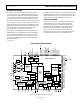
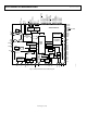
FUNCTIONAL BLOCK DIAGRAMS
I
PA
I
N
V
P
V
N
REF
IN/OUT
ENERGY
MEASUREMENT
DSP
OSC
COM0
...
...
COM3
.
.
.
CF1
CF2
3V/5V LCD
CHARGE PUMP
SINGLE
CYCLE
8052
MCU
ADE5166/ADE5169
V
DCIN
V
BAT
V
DD
V
SWOUT
DGND
AGND
LCDVA
LCDVB
LCDVC
.
.
.
FP0
FP15
RTC
SS
SCLK
MISO
MOSI/SDATA
T2
T2EX
T0
T1
LCDVP1
LCDVP2
XTAL2
XTAL1
INT0
INT1
FP16
FP17
FP23
FP22
FP21
FP20
FP19
FP18
FP25
FP24
1.20V
REF
52
53
49
50
I
PB
55
63
54
58
64
61
60
4647 48 45
5
6
FP28
FP27
2
1
7
8
9
10
11
12
13
14
20
35
1
4
15
17
18
16
19
44
14
13
12
57
43 42
39 38
7 6
45 11 43 42 41 40 39 38 37
36 5
6 7
8 9
1038
39 40
41
PGA2
–
+
PGA1
–
+
PGA1
–
+
ADC
ADC
ADC
TEMP
ADC
VSW
ADC
PROGRAM MEMORY
62kB FLASH
POWER SUPPLY
CONTROL AND
MONITORING
USER RAM
256 BYTES
USER XRAM
2kB
TEMP
SENSOR
BATTERY
ADC
SPI/I
2
C
SERIAL
INTERFACE
3 × 16-BIT
COUNTER
TIMERS
104-SEGMENT
LCD DRIVER
WATCHDOG
TIMER
PLL
07411-201
LDO
V
INTD
V
INTA
RESET
TxD
UART
SERIAL
PORT
UART2
SERIAL
PORT
UART2
TIMER
RxD
62
56
51
TxD2
44
36
RxD2
38
37
59
DOWNLOADER
DEBUGGER
1-PIN
EMULATOR
LDO
EA
UART
TIMER
POR
P0.7/SS/T1/RxD2
P0.6/SCLK/T0
P0.5/MISO/ZX
P0.4/MOSI/SDATA
P0.0 (BCTRL/INT1/P0.0)
P1.0/RxD
P1.1/TxD
P1.2/FP25/ZX
P1.3/T2EX/FP24
P1.6/FP21
P1.7/FP20
P1.4/T2/FP23
P1.5/FP22
P0.1/FP19
P0.2/CF1
P0.3/CF2
P2.0/FP18
P2.1/FP17
P2.2/FP16
P2.3 (SDEN/P2.3/TxD2)
Figure 1. ADE5166/ADE5169 Functional Block Diagram