Data Sheet Polyphase Multifunction Energy Metering IC with Harmonic and Fundamental Information ADE7854/ADE7858/ADE7868/ADE7878 FEATURES Highly accurate; supports EN 50470-1, EN 50470-3, IEC 62053-21, IEC 62053-22, and IEC 62053-23 standards Compatible with 3-phase, 3- or 4-wire (delta or wye), and other 3-phase services Supplies total (fundamental and harmonic) active, reactive (ADE7878, ADE7868, and ADE7858 only), and apparent energy, and fundamental active/reactive energy (ADE7878 only) on each phase a
ADE7854/ADE7858/ADE7868/ADE7878 Data Sheet TABLE OF CONTENTS Features .............................................................................................. 1 Power Quality Measurements................................................... 34 Applications ....................................................................................... 1 Phase Compensation ................................................................. 39 General Description ...............................................
Data Sheet ADE7854/ADE7858/ADE7868/ADE7878 REVISION HISTORY 10/13—Rev. F to Rev. G Changes to Product Title and Features Section ............................ 1 Changes to Table 2 ............................................................................ 9 Deleted Junction Temperature; Table 6 ........................................15 Changes to NC and CLKIN Pin Descriptions .............................16 Replaced Typical Performance Characteristics Section .............
ADE7854/ADE7858/ADE7868/ADE7878 No Load Detection Based On Total Active, Reactive Powers Section .............................................................................................. 61 Change to Equation 50................................................................... 63 Changes to the HSDC Interface Section ..................................... 70 Changes to Figure 87 and Figure 88 ............................................. 71 Changes to Figure 89 .........................................
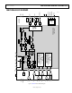
Figure 1. ADE7854 Functional Block Diagram Rev. G | Page 5 of 100 VN 18 VCP 19 ICN 14 ICP 13 VBP 22 IBN 12 IBP 9 VAP 23 IAN 8 IAP 7 CLKOUT 28 CLKIN 27 PGA1 PGA1 PGA1 PGA3 PGA3 PGA3 ADC ADC ADC ADC ADC ADC 17 4 1.
Rev. G | Page 6 of 100 Figure 2.
Rev. G | Page 7 of 100 Figure 3.
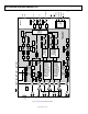
Rev. G | Page 8 of 100 Figure 4. ADE7878 Functional Block Diagram ICP INN 16 INP 15 VN 18 VCP 19 ICN 14 13 VBP 22 IBN 12 IBP 9 VAP 23 IAN 8 IAP 7 CLKOUT 28 CLKIN 27 PGA2 PGA1 PGA1 PGA1 PGA3 PGA3 PGA3 ADC ADC ADC ADC ADC ADC ADC 17 4 1.
Data Sheet ADE7854/ADE7858/ADE7868/ADE7878 SPECIFICATIONS VDD = 3.3 V ± 10%, AGND = DGND = 0 V, on-chip reference, CLKIN = 16.384 MHz, TMIN to TMAX = −40°C to +85°C, TTYP= 25°C. Table 2.
ADE7854/ADE7858/ADE7868/ADE7878 Parameter 1, 2 MEAN ABSOLUTE VALUE (MAV) MEASUREMENT (ADE7868 AND ADE7878) I mav Measurement Bandwidth (PSM1 Mode) I mav Measurement Error (PSM1 Mode) ANALOG INPUTS Maximum Signal Levels Input Impedance (DC) IAP, IAN, IBP, IBN, ICP, ICN, VAP, VBP, and VCP Pins VN Pin ADC Offset Min Typ Data Sheet Max Unit Test Conditions/Comments 260 Hz 0.
Data Sheet Parameter 1, 2 LOGIC OUTPUTS—IRQ0, IRQ1, MISO/HSD Output High Voltage, VOH ISOURCE Output Low Voltage, VOL ISINK CF1, CF2, CF3/HSCLK Output High Voltage, VOH ISOURCE Output Low Voltage, VOL ISINK POWER SUPPLY PSM0 Mode VDD Pin IDD PSM1 and PSM2 Modes (ADE7868 and ADE7878) VDD Pin IDD PSM1 Mode PSM2 Mode PSM3 Mode VDD Pin IDD in PSM3 Mode 1 2 ADE7854/ADE7858/ADE7868/ADE7878 Min Typ Max Unit 800 0.4 2 V µA V mA 500 0.4 2 V µA V mA 2.4 2.4 Test Conditions/Comments VDD = 3.
ADE7854/ADE7858/ADE7868/ADE7878 Data Sheet TIMING CHARACTERISTICS VDD = 3.3 V ± 10%, AGND = DGND = 0 V, on-chip reference, CLKIN = 16.384 MHz, TMIN to TMAX = −40°C to +85°C. Note that dual function pin names are referenced by the relevant function only within the timing tables and diagrams; see the Pin Configuration and Function Descriptions section for full pin mnemonics and descriptions. Table 3.
Data Sheet ADE7854/ADE7858/ADE7868/ADE7878 Table 4. SPI Interface Timing Parameters Parameter SS to SCLK Edge SCLK Period SCLK Low Pulse Width SCLK High Pulse Width Data Output Valid After SCLK Edge Data Input Setup Time Before SCLK Edge Data Input Hold Time After SCLK Edge Data Output Fall Time Data Output Rise Time SCLK Rise Time SCLK Fall Time MISO Disable After SS Rising Edge SS High After SCLK Edge Min 50 0.
ADE7854/ADE7858/ADE7868/ADE7878 Data Sheet Table 5.
Data Sheet ADE7854/ADE7858/ADE7868/ADE7878 ABSOLUTE MAXIMUM RATINGS TA = 25°C, unless otherwise noted. THERMAL RESISTANCE Table 6. θJA is specified equal to 29.3°C/W; θJC is specified equal to 1.8°C/W.
ADE7854/ADE7858/ADE7868/ADE7878 Data Sheet 40 39 38 37 36 35 34 33 32 31 NC SS/HSA MOSI/SDA MISO/HSD SCLK/SCL CF3/HSCLK CF2 CF1 IRQ1 NC PIN CONFIGURATION AND FUNCTION DESCRIPTIONS ADE78xx TOP VIEW (Not to Scale) 30 29 28 27 26 25 24 23 22 21 NC IRQ0 CLKOUT CLKIN VDD AGND AVDD VAP VBP NC NOTES 1. NC = NO CONNECT. 2. CREATE A SIMILAR PAD ON THE PCB UNDER THE EXPOSED PAD. SOLDER THE EXPOSED PAD TO THE PAD ON THE PCB TO CONFER MECHANICAL STRENGTH TO THE PACKAGE. CONNECT THE PADS TO AGND AND DGND.
Data Sheet Pin No. 18, 19, 22, 23 Mnemonic VN, VCP, VBP, VAP 24 AVDD 25 AGND 26 VDD 27 CLKIN 28 CLKOUT 29, 32 IRQ0, IRQ1 33, 34, 35 CF1, CF2, CF3/HSCLK 36 SCLK/SCL 37 38 39 EP MISO/HSD MOSI/SDA SS/HSA Exposed Pad ADE7854/ADE7858/ADE7868/ADE7878 Description Analog Inputs for the Voltage Channel. This channel is used with the voltage transducer and is referenced as the voltage channel in this document. These inputs are single-ended voltage inputs with a maximum signal level of ±0.
ADE7854/ADE7858/ADE7868/ADE7878 Data Sheet TYPICAL PERFORMANCE CHARACTERISTICS 1.5 VDD = 3.3V 1.2 0.9 0.6 0.6 0.3 0.3 ERROR (%) 0.9 0 –0.3 –0.9 –0.9 –1.2 –1.2 0.1 1 10 100 PERCENTAGE OF FULL-SCALE CURRENT (%) Figure 10. Total Active Energy Error As Percentage of Reading (Gain = +1, Power Factor = 1) over Temperature with Internal Reference and Integrator Off 0.15 0.10 –1.5 0.01 0.1 1 10 100 PERCENTAGE OF FULL-SCALE CURRENT (%) Figure 13.
1.5 3.63V 3.30V 2.97V 1.5 TA = 25°C 1.2 0.9 0.6 0.6 0.3 0.3 ERROR (%) 0.9 0 –0.3 –0.9 –0.9 –1.2 –1.2 0.1 1 10 100 PERCENTAGE OF FULL-SCALE CURRENT (%) Figure 16. Total Reactive Energy Error As Percentage of Reading (Gain = +1, Power Factor = 0) over Power Supply with Internal Reference and Integrator Off 1.5 1.2 +85°C +25°C –40°C –1.5 0.01 0.1 1 10 100 PERCENTAGE OF FULL-SCALE CURRENT (%) Figure 19.
ADE7854/ADE7858/ADE7868/ADE7878 1.5 1.2 +85°C +25°C –40°C Data Sheet VDD = 3.3V 0.9 ERROR (%) 0.6 0.3 0 –0.3 –0.6 –0.9 –1.5 0.01 0.1 1 10 PERCENTAGE OF FULL-SCALE CURRENT (%) 100 08510-613 –1.2 Figure 22. IRMS Error as Percentage of Reading (Gain = +1, Power Factor = 1) over Temperature with Internal Reference and Integrator Off Rev.
Data Sheet ADE7854/ADE7858/ADE7868/ADE7878 TEST CIRCUIT Note that in Figure 23, the PM1 and PM0 pins are pulled up internally to 3.3 V. Select the mode of operation by using a microcontroller to programmatically change the pin values. 3.3V 10µF 1kΩ 10kΩ 1µF 0.22µF PM0 3 PM1 24 26 5 DVDD 2 0.1µF 4.7µF VDD 3.3V + AVDD 4.7µF + + 0.22µF SS/HSA 39 MOSI/SDA 38 4 RESET 22nF 7 IAP 22nF 8 IAN 9 IBP MISO/HSD 37 3.
ADE7854/ADE7858/ADE7868/ADE7878 Data Sheet TERMINOLOGY Measurement Error The error associated with the energy measurement made by the ADE7854/ADE7858/ADE7868/ADE7878 is defined by Measurement Error = Energy Registered by ADE78 xx − True Energy True Energy × 100% (1) Power Supply Rejection (PSR) This quantifies the ADE7854/ADE7858/ADE7868/ADE7878 measurement error as a percentage of reading when the power supplies are varied. For the ac PSR measurement, a reading at nominal supplies (3.3 V) is taken.
Data Sheet ADE7854/ADE7858/ADE7868/ADE7878 POWER MANAGEMENT The ADE7868/ADE7878 have four modes of operation, determined by the state of the PM0 and PM1 pins (see Table 9). The ADE7854/ADE7858 have two modes of operation. These pins provide complete control of the ADE7854/ADE7858/ADE7868/ ADE7878 operation and can easily be connected to an external microprocessor I/O. The PM0 and PM1 pins have internal pullup resistors.
ADE7854/ADE7858/ADE7868/ADE7878 Data Sheet The threshold is derived from Bits[2:0] (LPOIL[2:0]) of the LPOILVL register as LPOIL[2:0]/8 of full scale. Every time one phase current becomes greater than the threshold, a counter is incremented. If every phase counter remains below LPLINE[4:0] + 1 at the end of the measurement period, then the IRQ0 pin is triggered low. If a single phase counter becomes greater or equal to LPLINE[4:0] + 1 at the end of the measurement period, the IRQ1 pin is triggered low.
Data Sheet ADE7854/ADE7858/ADE7868/ADE7878 Table 11.
ADE7854/ADE7858/ADE7868/ADE7878 Data Sheet POWER-UP PROCEDURE 3.3V – 10% 2.0V ± 10% ADE78xx PSM0 READY 0V ADE78xx POWERED UP POR TIMER TURNED ON 40ms MICROPROCESSOR MAKES THE ADE78xx MICROPROCESSOR RSTDONE CHOICE BETWEEN ENTER PSM3 INTERRUPT I2C AND SPI SETS ADE78xx TRIGGERED IN PSM0 08510-009 26ms Figure 26. Power-Up Procedure The ADE7854/ADE7858/ADE7868/ADE7878 contain an onchip power supply monitor that supervises the power supply (VDD).
Data Sheet ADE7854/ADE7858/ADE7868/ADE7878 HARDWARE RESET SOFTWARE RESET FUNCTIONALITY The ADE7854/ADE7858/ADE7868/ADE7878 each has a RESET pin. If the ADE7854, ADE7858, ADE7868, or ADE7878 is in PSM0 mode and the RESET pin is set low, then the ADE78xx enters the hardware reset state. The ADE78xx must be in PSM0 mode for a hardware reset to be considered. Setting the RESET pin low while the ADE78xx is in PSM1, PSM2, and PSM3 modes does not have any effect.
ADE7854/ADE7858/ADE7868/ADE7878 Data Sheet THEORY OF OPERATION DIFFERENTIAL INPUT V1 + V2 = 500mV MAX PEAK COMMON MODE VCM = ±25mV MAX V1 + V2 +500mV V1 IAP, IBP, ICP, OR INP V2 IAN, IBN, ICN, OR INN VCM –500mV 08510-010 VCM Figure 27. Maximum Input Level, Current Channels, Gain = 1 All inputs have a programmable gain amplifier (PGA) with a possible gain selection of 1, 2, 4, 8, or 16. The gain of IA, IB, and IC inputs is set in Bits[2:0] (PGA1[2:0]) of the gain register.
ADE7854/ADE7858/ADE7868/ADE7878 the bandwidth of interest. For example, the sampling rate in the ADE7854/ADE7858/ADE7868/ADE7878 is 1.024 MHz, and the bandwidth of interest is 40 Hz to 2 kHz. Oversampling has the effect of spreading the quantization noise (noise due to sampling) over a wider bandwidth. With the noise spread more thinly over a wider bandwidth, the quantization noise in the band of interest is lowered, as shown in Figure 31.
ADE7854/ADE7858/ADE7868/ADE7878 Data Sheet LPF1 0x5A7540 = +5,928,256 CURRENT PEAK, OVERCURRENT DETECT INTEN BIT CONFIG[0] DSP IAP VIN PGA1 BITS REFERENCE GAIN[2:0] ×1, ×2, ×4, ×8, ×16 PGA1 HPFDIS [23:0] ADC ZX SIGNAL DATA RANGE ZX DETECTION 0V CURRENT RMS (IRMS) CALCULATION DIGITAL INTEGRATOR IAWV WAVEFORM SAMPLE REGISTER AIGAIN[23:0] 0xA58AC0 = –5,928,256 TOTAL/FUNDAMENTAL ACTIVE AND REACTIVE POWER CALCULATION HPF IAN CURRENT CHANNE L DATA RANGE AFTER INTEGRATION CURRENT CHANNE L DATA
Data Sheet ADE7854/ADE7858/ADE7868/ADE7878 Current Channel Sampling The waveform samples of the current channel are taken at the output of HPF and stored in the 24-bit signed registers, IAWV, IBWV, ICWV, and INWV (ADE7868 and ADE7878 only) at a rate of 8 kSPS. All power and rms calculations remain uninterrupted during this process. Bit 17 (DREADY) in the STATUS0 register is set when the IAWV, IBWV, ICWV, and INWV registers are available to be read using the I2C or SPI serial port.
ADE7854/ADE7858/ADE7868/ADE7878 Data Sheet register with four MSBs padded with 0s and sign extended to 28 bits, which practically means it is transmitted equal to 0xFFF8000. –20 –25 –30 30 35 40 45 50 55 FREQUENCY (Hz) 60 65 When the digital integrator is switched off, the ADE7854/ ADE7858/ ADE7868/ADE7878 can be used directly with a conventional current sensor, such as a current transformer (CT).
Data Sheet ADE7854/ADE7858/ADE7868/ADE7878 Voltage Waveform Gain Registers CHANGING PHASE VOLTAGE DATAPATH There is a multiplier in the signal path of each phase voltage. The voltage waveform can be changed by ±100% by writing a corresponding twos complement number to the 24-bit signed voltage waveform gain registers (AVGAIN, BVGAIN, and CVGAIN). For example, if 0x400000 is written to those registers, the ADC output is scaled up by 50%. To scale the input by −50%, write 0xC00000 to the registers.
ADE7854/ADE7858/ADE7868/ADE7878 Data Sheet IA DSP VTOIB[1:0] = 10, PHASE A VOLTAGE DIRECTED TO PHASE B VA IB BPHCAL PGA ADC HPF 0V IA, IB, IC, OR VA, VB, VC PHASE C COMPUTATIONAL DATAPATH LPF1 39.6° OR 2.2ms @ 50Hz ZX ZX ZX ZX LPF1 OUTPUT Figure 43. Zero-Crossing Detection on Voltage and Current Channels VTOIA[1:0] = 10, PHASE C VOLTAGE DIRECTED TO PHASE A 08510-026 VC xIGAIN[23:0] OR xVGAIN[23:0] 1 0.
Data Sheet ADE7854/ADE7858/ADE7868/ADE7878 Figure 44 shows the mechanism of the zero-crossing timeout detection when the voltage or the current signal stays at a fixed dc level for more than 62.5 μs × ZXTOUT μs. 16-BIT INTERNAL REGISTER VALUE ZXTOUT PHASE A PHASE C PHASE B A, B, C PHASE VOLTAGES AFTER LPF1 ZX A ZX C ZX B BIT 19 (SEQERR) IN STATUS1 REGISTER 0V STATUS1[19] SET TO 1 ZXZOxy FLAG IN STATUS1[31:0], x = V, A y = A, B, C Figure 45.
ADE7854/ADE7858/ADE7868/ADE7878 PHASE A VOLTAGE Data Sheet LPF1 filter (see Figure 43), a settling time of 30 ms to 40 ms is associated with this filter before the measurement is stable. 08510-031 PHASE A CURRENT ANGLE0 Figure 47. Delay Between Phase A Voltage and Phase A Current Is Stored in the ANGLE0 Register When the ANGLESEL[1:0] bits are set to 01, the delays between phase voltages are measured. The delay between Phase A voltage and Phase C voltage is stored into the ANGLE0 register.
ADE7854/ADE7858/ADE7868/ADE7878 Figure 49. SAG Detection Figure 49 shows Phase A voltage falling below a threshold that is set in the SAG level register (SAGLVL) for four half-line cycles (SAGCYC = 4). When Bit 16 (SAG) in the STATUS1 register is set to 1 to indicate the condition, Bit VSPHASE[0] in the PHSTATUS register is also set to 1 because the event happened on Phase A Bit 16 (SAG) in the STATUS1 register.
ADE7854/ADE7858/ADE7868/ADE7878 PEAK VALUE WRITTEN INTO IPEAK AT THE END OF FIRST PEAKCYC PERIOD thereby ensuring that the first peak detection result is obtained across a full PEAKCYC period.
5. ADE7854/ADE7858/ADE7868/ADE7878 The STATUS1 register is written with Bit 18 (OV) set to 1. In this moment, Bit OV is erased and also all Bits[11:9] (OVPHASE[2:0]) of the PHSTATUS register. In case of an overcurrent event, if Bit 17 (OI) in the MASK1 register is set, the IRQ1 interrupt pin is driven low. Immediately, Bit 17 (OI) in the STATUS1 register and one of Bits[5:3] (OIPHASE[2:0]) in the PHSTATUS register, which identify the phase that generated the interrupt, are set.
ADE7854/ADE7858/ADE7868/ADE7878 Data Sheet phase errors. For example, a current transformer (CT) with a phase error of 0.1° to 3° is not uncommon. These phase errors can vary from part to part, and they must be corrected to perform accurate power calculations. acceptable; numbers outside this range are not accepted. If the current leads the voltage, the result is negative and the absolute value is written into the PHCAL registers.
Data Sheet ADE7854/ADE7858/ADE7868/ADE7878 REFERENCE CIRCUIT The nominal reference voltage at the REFIN/OUT pin is 1.2 V. This is the reference voltage for the ADCs in the ADE7854/ ADE7858/ADE7868/ADE7878. Use a typical external reference voltage of 1.2 V to overdrive the REFIN/OUT pin. The temperature coefficient of the internal voltage reference is calculated based on the endpoint method.
ADE7854/ADE7858/ADE7868/ADE7878 Data Sheet –50 –45 –40 –35 –30 –5 –20 –15 –10 –5 0 5 10 15 20 25 30 35 40 45 50 HOT TEMPERATURE COEFFICIENT (ppm/°C) 08510-257 NUMBER OF PARTS memory RAM are initialized at 0, their default values, and they can be read/written without any restriction. The run register, used to start and stop the DSP, is cleared to 0x0000. The run register needs to be written with 0x0001 for the DSP to start code execution. Figure 58.
Data Sheet ADE7854/ADE7858/ADE7868/ADE7878 an internal 8-bit register located at Address 0xE7FE, followed by a write of 0x00 to an internal 8-bit register located at Address 0xE7E3. Reinitialize the registers. Write the last register in the queue three times. Enable the write protection by writing 0xAD to an internal 8-bit register located at Address 0xE7FE, followed by a write of 0x80 to an internal 8-bit register located at Address 0xE7E3.
ADE7854/ADE7858/ADE7868/ADE7878 Data Sheet power-up and DSP reset cases, it would typically take about 1.2 seconds for a FS/1000 signal to be settled. the integrator is enabled, that is, when Bit 0 (INTEN) in the CONFIG register is set to 1, the equivalent rms value of a fullscale sinusoidal signal at 50 Hz is 4,191,910 (0x3FF6A6) and at 60 Hz is 3,493,258 (0x354D8A). Table 13.
ADE7854/ADE7858/ADE7868/ADE7878 Current RMS Offset Compensation 212000 The ADE7854/ADE7858/ADE7868/ADE7878 incorporate a current rms offset compensation register for each phase: AIRMSOS, BIRMSOS, CIRMSOS registers, and the NIRMSOS register for ADE7868 and ADE7878 only. These are 24-bit signed registers that are used to remove offsets in the current rms calculations. An offset can exist in the rms calculation due to input noises that are integrated in the dc component of I2(t).
ADE7854/ADE7858/ADE7868/ADE7878 Data Sheet values and they are stored into the Registers AVRMS, BVRMS, and CVRMS. The update rate of the current rms measurement is 8 kHz. to ensure stability. The IRQ1 interrupt can be used to indicate when a zero crossing has occurred (see the Interrupts section). With the specified full-scale analog input signal of 0.5 V, the ADC produces an output code that is approximately ±5,928,256.
Data Sheet ADE7854/ADE7858/ADE7868/ADE7878 Voltage RMS Offset Compensation The ADE78xx incorporates voltage rms offset compensation registers for each phase: AVRMSOS, BVRMSOS, and CVRMSOS. These are 24-bit signed registers used to remove offsets in the voltage rms calculations. An offset can exist in the rms calculation due to input noises that are integrated in the dc component of V2(t).
ADE7854/ADE7858/ADE7868/ADE7878 Data Sheet If the phase currents and voltages contain only the fundamental component, are in phase (that is φ1 = γ1 = 0), and they correspond to full-scale ADC inputs, then multiplying them results in an instantaneous power signal that has a dc component, V1 × I1, and a sinusoidal component, V1 × I1 cos(2ωt); Figure 65 shows the corresponding waveforms.
Data Sheet ADE7854/ADE7858/ADE7868/ADE7878 The output is scaled by −50% by writing 0xC00000 to the watt gain registers, and it is increased by +50% by writing 0x400000 to them. These registers are used to calibrate the active power (or energy) calculation in the ADE7854/ADE7858/ADE7868/ ADE7878for each phase. As stated in the Current Waveform Gain Registers section, the serial ports of the ADE7854/ADE7858/ADE7868/ADE7878 work on 32-, 16-, or 8-bit words, and the DSP works on 28 bits.
ADE7854/ADE7858/ADE7868/ADE7878 HPFDIS [23:0] Data Sheet DIGITAL INTEGRATOR AIGAIN REVAPA BIT IN STATUS0[31:0] IA HPF APHCAL AWGAIN HPFDIS [23:0] AWATTOS AWATTHR[31:0] AVGAIN ACCUMULATOR LPF2 32-BIT REGISTER VA HPF WTHR[47:0] 08510-044 AWATT 24 DIGITAL SIGNAL PROCESSOR Figure 67. Total Active Energy Accumulation The ADE7854/ADE7858/ADE7868/ADE7878 achieve the integration of the active power signal in two stages (see Figure 67).
Data Sheet ADE7854/ADE7858/ADE7868/ADE7878 CFWATTHR 32-bit signed registers. The active energy register content can roll over to full-scale negative (0x80000000) and continue increasing in value when the active power is positive. Conversely, if the active power is negative, the energy register underflows to full-scale positive (0x7FFFFFFF) and continues decreasing in value. Table 15.
ADE7854/ADE7858/ADE7868/ADE7878 Data Sheet Because the active power is integrated on an integer number of half-line cycles in this mode, the sinusoidal components are reduced to 0, eliminating any ripple in the energy calculation.
Data Sheet ADE7854/ADE7858/ADE7868/ADE7878 Note that q(t) can be rewritten as ∞ { q(t ) = ∑ Vk I k cos(φk − γk − k =1 ∞ ∑ V kI m k ,m =1 k ≠m π 2 ) − cos(2 kωt + φ + γ + π )} + k k 2 Table 17. Settling Time for Fundamental Reactive Power {cos[(k – m)ωt + φ − γ − π2 ]− k cos[(k + m)ωt + φk + γk + π 2 k ]} 63% Full Scale 375 ms (32) The average total reactive power over an integral number of line cycles (n) is given by the expression in Equation 33.
ADE7854/ADE7858/ADE7868/ADE7878 Sign of Reactive Power Calculation Note that the reactive power is a signed calculation. Table 18 summarizes the relationship between the phase difference between the voltage and the current and the sign of the resulting reactive power calculation. The ADE7858/ADE7868/ADE7878 have sign detection circuitry for reactive power calculations that can monitor the total reactive powers or the fundamental reactive powers.
Data Sheet ADE7854/ADE7858/ADE7868/ADE7878 Bit 2 (REHF) in the STATUS0 register is set when Bit 30 of one of the xVARHR registers changes, signifying one of these registers is half full. If the reactive power is positive, the var-hour register becomes half full when it increments from 0x3FFF FFFF to 0x4000 0000. If the reactive power is negative, the var-hour register becomes half full when it decrements from 0xC000 0000 to 0xBFFF FFFF.
ADE7854/ADE7858/ADE7868/ADE7878 Integration Time Under A Steady Load The discrete time sample period (T) for the accumulation register is 125 µs (8 kHz frequency). With full-scale pure sinusoidal signals on the analog inputs and a 90° phase difference between the voltage and the current signal (the largest possible reactive power), the average word value representing the reactive power is PMAX = 33,516,139 = 0x1FF6A6B.
Data Sheet ADE7854/ADE7858/ADE7868/ADE7878 The ADE7854/ADE7858/ADE7868/ADE7878 store the instantaneous phase apparent powers into the AVA, BVA, and CVA registers. Their expression is APPARENT POWER CALCULATION Apparent power is defined as the maximum power that can be delivered to a load. One way to obtain the apparent power is by multiplying the voltage rms value by the current rms value (also called the arithmetic apparent power) S = V rms × I rms xVA = (39) where: S is the apparent power.
ADE7854/ADE7858/ADE7868/ADE7878 Apparent Power Gain Calibration The average apparent power result in each phase can be scaled by ±100% by writing to one of the phase’s VAGAIN 24-bit registers (AVAGAIN, BVAGAIN, or CVAG AIN). The VAGAIN registers are twos complement, signed registers and have a resolution of 2−23/LSB.
Data Sheet ADE7854/ADE7858/ADE7868/ADE7878 In the ADE7854/ADE7858/ADE7868/ADE7878, the phase apparent powers are accumulated in the AVAHR, BVAHR, and CVAHR 32-bit signed registers. The apparent energy register content can roll over to full-scale negative (0x80000000) and continue increasing in value when the apparent power is positive. The maximum value that can be stored in the xVAHR accumulation register before it overflows is 231 − 1 or 0x7FFFFFFF.
ADE7854/ADE7858/ADE7868/ADE7878 The line cycle apparent energy accumulation mode is activated by setting Bit 2 (LVA) in the LCYCMODE register. The apparent energy accumulated over an integer number of zero crossings is written to the xVAHR accumulation registers after the number of zero crossings specified in LINECYC register is detected.
Data Sheet ADE7854/ADE7858/ADE7868/ADE7878 Table 22. CFxSEL Bits Description Second, Bits[2:0] (CF1SEL[2:0]), Bits[5:3] (CF2SEL[2:0]), and Bits[8:6] (CF3SEL[2:0]) in the CFMODE register decide what type of power is used at the inputs of the CF1, CF2, and CF3 converters, respectively.
ADE7854/ADE7858/ADE7868/ADE7878 The second stage consists of the frequency divider by the CFxDEN 16-bit unsigned registers. The values of CFxDEN depend on the meter constant (MC), measured in impulses/kWh and how much energy is assigned to one LSB of various energy registers: xWATTHR, xVARHR, and so forth. Supposing a derivative of wh [10n wh], n a positive or negative integer, is desired as one LSB of xWATTHR register.
Data Sheet ADE7854/ADE7858/ADE7868/ADE7878 CF Outputs for Various Accumulation Modes Bits[1:0] (WATTACC[1:0]) in the ACCMODE register determine the accumulation modes of the total active and fundamental powers when signals proportional to the active powers are chosen at the CFx pins (the CFxSEL[2:0] bits in the CFMODE register equal 000 or 011). When WATTACC[1:0] = 00 (the default value), the active powers are sign accumulated before entering the energyto-frequency converter.
ADE7854/ADE7858/ADE7868/ADE7878 Data Sheet NO LOAD CONDITION The no load condition is defined in metering equipment standards as occurring when the voltage is applied to the meter and no current flows in the current circuit.
Data Sheet ADE7854/ADE7858/ADE7868/ADE7878 of Phase B, and NLPHASE[2] indicates the state of Phase C. When Bit NLPHASE[x] is cleared to 0, it means the phase is out of a no load condition. When set to 1, it means the phase is in a no load condition. An interrupt attached to Bit 0 (NLOAD) in the STATUS1 register can be enabled by setting Bit 0 in the MASK1 register. If enabled, the IRQ1 pin is set to low, and the status bit is set to 1 whenever one of three phases enters or exits this no load condition.
ADE7854/ADE7858/ADE7868/ADE7878 Data Sheet gi, i = 0, 1, 2, …, 31 are the coefficients of the generating polynomial defined by the IEEE802.3 standard as follows: default values. The ADE78xx computes the cyclic redundancy check (CRC) based on the IEEE802.3 standard. The registers are introduced one-by-one into a linear feedback shift register (LFSR) based generator starting with the least significant bit (as shown in Figure 82). The 32-bit result is written in the CHECKSUM register.
Data Sheet ADE7854/ADE7858/ADE7868/ADE7878 goes active low. The flag bits in the interrupt status register are set irrespective of the state of the mask bits. To determine the source of the interrupt, the MCU should perform a read of the corresponding STATUSx register and identify which bit is set to 1. To erase the flag in the status register, write back to the STATUSx register with the flag set to 1.
ADE7854/ADE7858/ADE7868/ADE7878 t1 Data Sheet t2 t3 MCU INTERRUPT FLAG SET PROGRAM SEQUENCE GLOBAL INTERRUPT MASK JUMP TO ISR CLEAR MCU INTERRUPT FLAG READ STATUSx WRITE BACK STATUSx ISR ACTION (BASED ON STATUSx CONTENTS) ISR RETURN GLOBAL INTERRUPT MASK RESET JUMP TO ISR 08510-057 IRQx Figure 84.
Data Sheet ADE7854/ADE7858/ADE7868/ADE7878 I2C Write Operation The write operation using the I2C interface of the ADE7854/ ADE7858/ADE7868/ADE7878 initiate when the master generates a start condition and consists in one byte representing the address of the ADE78xx followed by the 16-bit address of the target register and by the value of the register.
ADE7854/ADE7858/ADE7868/ADE7878 Data Sheet I2C Read Operation ADE7854/ADE7858/ADE7868/ADE7878, the second stage begins with the master generating a new start condition followed by an address byte. The most significant seven bits of this address byte constitute the address of the ADE78xx, and they are equal to 0111000b. Bit 0 of the address byte is a read/write bit. Because this is a read operation, it must be set to 1; thus, the first byte of the read operation is 0x71.
Data Sheet ADE7854/ADE7858/ADE7868/ADE7878 SPI-Compatible Interface The SS logic input is the chip select input. This input is used when multiple devices share the serial bus. Drive the SS input low for the entire data transfer operation. Bringing SS high during a data transfer operation aborts the transfer and places the serial bus in a high impedance state. A new transfer can then be initiated by returning the SS logic input to low.
ADE7854/ADE7858/ADE7868/ADE7878 Data Sheet SPI Write Operation The write operation using the SPI interface of the ADE78xx initiates when the master sets the SS/HSA pin low and begins sending one byte representing the address of the ADE7854/ ADE7858/ADE7868/ADE7878 on the MOSI line. The master sets data on the MOSI line starting with the first high-to-low transition of SCLK. The SPI of the ADE78xx samples data on the low-to-high transitions of SCLK.
Data Sheet ADE7854/ADE7858/ADE7868/ADE7878 HSDC Interface The high speed data capture (HSDC) interface is disabled after default. It can be used only if the ADE7854/ADE7858/ADE7868/ ADE7878 is configured with an I2C interface. The SPI interface of the ADE7854/ADE7858/ADE7868/ADE7878 cannot be used simultaneously with HSDC. Bit 6 (HSDCEN) in the CONFIG register activates HSDC when set to 1. If Bit HSDCEN is cleared to 0, the default value, the HSDC interface is disabled.
ADE7854/ADE7858/ADE7868/ADE7878 Data Sheet Figure 93 shows the HSDC transfer protocol for HSIZE = 0, HGAP = 1, HXFER[1:0] = 00, and HSAPOL = 0. Note that the HSDC interface introduces a seven-HSCLK cycles gap between every 32-bit word. Table 24 lists the time it takes to execute an HSDC data transfer for all HSDC_CFG register settings. For some settings, the transfer time is less than 125 μs (8 kHz), the waveform sample registers update rate. This means the HSDC port transmits data every sampling cycle.
Data Sheet ADE7854/ADE7858/ADE7868/ADE7878 HSCLK 31 HSD 24 23 IAVW (BYTE 3) 16 15 IAWV (BYTE 2) 8 7 IAWV (BYTE 1) 0 CVAR (BYTE 0) 7 HCLK CYCLES 08510-068 7 HCLK CYCLES HSA Figure 94. HSDC Communication for HSIZE = 1, HGAP = 1, HXFER[1:0] = 00, and HSAPOL = 0 C2 0.22µF C5 0.
ADE7854/ADE7858/ADE7868/ADE7878 Data Sheet shown in Figure 98. CL1 and CL2 denote the capacitances of the ceramic capacitors attached to the crystal pins, whereas CP1 and CP2 denote the parasitic capacitances on those pins. The recommended typical value of total capacitance at each clock pin, CLKIN and CLKOUT, is 24 pF, which means that Total Capacitance = CP1 + CL1 = CP2 + CL2 = 24 pF Crystal manufacturer data sheets specify the load capacitance value.
Data Sheet ADE7854/ADE7858/ADE7868/ADE7878 SILICON ANOMALY This anomaly list describes the known issues with the ADE7854, ADE7858, ADE7868, and ADE7878 silicon identified by the version register (Address 0xE707) being equal to 2, to 4, and to 5. Analog Devices, Inc., is committed, through future silicon revisions, to continuously improve silicon functionality.
ADE7854/ADE7858/ADE7868/ADE7878 Data Sheet Table 26. Values Written to the CF1DEN, CF2DEN, CF3DEN, SAGLVL, and ZXTOUT Registers May Not Be Immediately Used By ADE7854, ADE7858, ADE7868, ADE7878 [er002, Version = 2 Silicon] Background Issue Workaround Related Issues Usually, the CF1DEN, CF2DEN, CF3DEN, SAGLVL, and ZXTOUT registers initialize immediately after power-up or after a hardware/software reset.
Data Sheet ADE7854/ADE7858/ADE7868/ADE7878 Table 29. Values Written to the SAGLVL and ZXTOUT Registers May Not Be Immediately Used by ADE7854, ADE7858, ADE7868, and ADE7878 [er005, Version = 4 and Version = 5 Silicons] Background Issue Workaround Related Issues Usually, the SAGLVL and ZXTOUT registers initialize immediately after power-up or after a hardware/software reset.
ADE7854/ADE7858/ADE7868/ADE7878 Data Sheet REGISTERS LIST Table 30.
Data Sheet ADE7854/ADE7858/ADE7868/ADE7878 Address 0x43A3 Register Name AFVARGAIN R/W 1 R/W Bit Length 24 Bit Length During Communication 2 32 ZPSE Type 3 S Default Value 0x000000 0x43A4 AFVAROS R/W 24 32 ZPSE S 0x000000 0x43A5 BFVARGAIN R/W 24 32 ZPSE S 0x000000 0x43A6 BFVAROS R/W 24 32 ZPSE S 0x000000 0x43A7 CFVARGAIN R/W 24 32 ZPSE S 0x000000 0x43A8 CFVAROS R/W 24 32 ZPSE S 0x000000 0x43A9 VATHR1 R/W 24 32 ZP U 0x000000 0x43AA VATHR0 R/W 24 32 ZP U
ADE7854/ADE7858/ADE7868/ADE7878 Data Sheet Register Name Reserved R/W 1 N/A4 Bit Length N/A4 Bit Length During Communication 2 N/A4 Type 3 N/A4 Default Value 0x000000 ISUM R 28 32 ZP S N/A4 0x43C0 0x43C1 0x43C2 0x43C3 0x43C4 0x43C5 0x43C6 AIRMS AVRMS BIRMS BVRMS CIRMS CVRMS NIRMS R R R R R R R 24 24 24 24 24 24 24 32 ZP 32 ZP 32 ZP 32 ZP 32 ZP 32 ZP 32 ZP S S S S S S S N/A4 N/A4 N/A4 N/A4 N/A4 N/A4 N/A4 0x43C7 to 0x43FF Reserved N/A4 N/A4 N/A4 N/A4 N/A4 Address 0x43B9 to 0x43BE 0
Data Sheet Address 0xE40C 0xE40D 0xE40E 1 2 3 Register Name AVAHR BVAHR CVAHR ADE7854/ADE7858/ADE7868/ADE7878 R/W 1, 2 R R R Bit Length2 32 32 32 Bit Length During Communication2 32 32 32 Type2, 3 S S S Default Value 0x00000000 0x00000000 0x00000000 Description Phase A apparent energy accumulation. Phase B apparent energy accumulation. Phase C apparent energy accumulation. R is read, and W is write. N/A is not applicable. U is unsigned register, and S is signed register in twos complement format.
ADE7854/ADE7858/ADE7868/ADE7878 Data Sheet R/W 1 R Bit Length 24 Bit Length During Communication 2 32 SE Type 3 S Default Value 4 N/A BVA R 24 32 SE S N/A 0xE51B CVA R 24 32 SE S N/A 0xE51F CHECKSUM R 32 32 U 0x33666787 0xE520 VNOM R/W 24 32 ZP S 0x000000 0xE521 to 0xE52E 0xE600 0xE601 Reserved PHSTATUS ANGLE0 R R 16 16 16 16 U U N/A N/A 0xE602 ANGLE1 R 16 16 U N/A 0xE603 ANGLE2 R 16 16 U N/A 0xE604 to 0xE606 0xE607 0xE608 0xE609 to 0xE60B 0xE60C 0xE60D
Data Sheet ADE7854/ADE7858/ADE7868/ADE7878 Bit Length 8 Bit Length During Communication 2 8 Address 0xE705 Register Name CFCYC 0xE706 0xE707 0xEBFF HSDC_CFG Version Reserved R/W R 8 8 8 8 8 8 U U 0x00 0xEC00 LPOILVL R/W 8 8 U 0x07 0xEC01 CONFIG2 R/W 8 8 U 0x00 R/W 1 R/W Type 3 U Default Value 4 0x01 Description Number of CF pulses between two consecutive energy latches. See the Synchronizing Energy Registers with CFx Outputs section. HSDC configuration register. See Table 53.
ADE7854/ADE7858/ADE7868/ADE7878 Bit Location 3 Bit Mnemonic FREHF Default Value 0 4 VAEHF 0 5 LENERGY 0 6 REVAPA 0 7 REVAPB 0 8 REVAPC 0 9 REVPSUM1 0 10 REVRPA 0 11 REVRPB 0 12 REVRPC 0 13 REVPSUM2 0 14 CF1 15 CF2 16 CF3 17 DREADY 0 18 REVPSUM3 0 31:19 Reserved 0 0000 0000 0000 Data Sheet Description When this bit is set to 1, it indicates that Bit 30 of any one of the fundamental reactive energy registers, AFVARHR, BFVARHR, or CFVARHR, has changed.
Data Sheet ADE7854/ADE7858/ADE7868/ADE7878 Table 38.
ADE7854/ADE7858/ADE7868/ADE7878 Data Sheet Table 39.
Data Sheet ADE7854/ADE7858/ADE7868/ADE7878 Table 40.
ADE7854/ADE7858/ADE7868/ADE7878 Data Sheet Table 41. PHSTATUS Register (Address 0xE600) Bit Location 2:0 3 4 5 8:6 9 10 11 12 13 14 15 Bit Mnemonic Reserved OIPHASE[0] OIPHASE[1] OIPHASE[2] Reserved OVPHASE[0] OVPHASE[1] OVPHASE[2] VSPHASE[0] VSPHASE[1] VSPHASE[2] Reserved Default Value 000 0 0 0 000 0 0 0 0 0 0 0 Description Reserved. These bits are always 0. When this bit is set to 1, Phase A current generates Bit 17 (OI) in the STATUS1 register.
Data Sheet ADE7854/ADE7858/ADE7868/ADE7878 Table 43. COMPMODE Register (Address 0xE60E) Bit Location 0 Bit Mnemonic TERMSEL1[0] Default Value 1 1 2 3 TERMSEL1[1] TERMSEL1[2] TERMSEL2[0] 1 1 1 4 5 6 TERMSEL2[1] TERMSEL2[2] TERMSEL3[0] 1 1 1 7 8 10:9 TERMSEL3[1] TERMSEL3[2] ANGLESEL[1:0] 1 1 00 11 VNOMAEN 0 12 VNOMBEN 0 13 VNOMCEN 0 14 SELFREQ 0 15 Reserved 0 Description Setting all TERMSEL1[2:0] to 1 signifies the sum of all three phases is included in the CF1 output.
ADE7854/ADE7858/ADE7868/ADE7878 8:6 PGA3[2:0] 000 15:9 Reserved 000 0000 Data Sheet Phase voltages gain selection. 000: gain = 1. 001: gain = 2. 010: gain = 4. 011: gain = 8. 100: gain = 16. 101, 110, 111: reserved. When set, the ADE7854/ADE7858/ADE7868/ADE7878 behave like PGA3[2:0] = 000. Reserved. These bits do not manage any functionality. Table 45.
Data Sheet ADE7854/ADE7858/ADE7868/ADE7878 Bit Location 10 Bit Mnemonic CF2DIS Default Value 1 11 CF3DIS 1 12 CF1LATCH 0 13 CF2LATCH 0 14 CF3LATCH 0 15 Reserved 0 Description When this bit is set to 1, the CF2 output is disabled. The respective digital to frequency converter remains enabled even if CF2DIS = 1. When this bit is set to 0, the CF2 output is enabled. When this bit is set to 1, the CF3 output is disabled.
ADE7854/ADE7858/ADE7868/ADE7878 Bit Location 7 Bit Mnemonic SUM2SIGN Default Value 0 8 SUM3SIGN 0 15:9 Reserved 000 0000 Data Sheet Description 0: if the sum of all phase powers in the CF2 datapath is positive. 1: if the sum of all phase powers in the CF2 datapath is negative. Phase powers in the CF2 datapath are identified by Bits[5:3] (TERMSEL2[x]) of the COMPMODE register and by Bits[5:3] (CF2SEL[x]) of the CFMODE register. 0: if the sum of all phase powers in the CF3 datapath is positive.
Data Sheet ADE7854/ADE7858/ADE7868/ADE7878 Table 49. MMODE Register (Address 0xE700) Bit Location 1:0 Bit Mnemonic PERSEL[1:0] Default Value 00 2 PEAKSEL[0] 1 3 4 7:5 PEAKSEL[1] PEAKSEL[2] Reserved 1 1 000 Description 00: Phase A selected as the source of the voltage line period measurement. 01: Phase B selected as the source of the voltage line period measurement. 10: Phase C selected as the source of the voltage line period measurement. 11: reserved.
ADE7854/ADE7858/ADE7868/ADE7878 Data Sheet Table 51.
Data Sheet ADE7854/ADE7858/ADE7868/ADE7878 Bit Location 4:3 Bit Mnemonic HXFER[1:0] Default Value 00 5 HSAPOL 0 7:6 Reserved 00 Description 00 = for ADE7854, HSDC transmits sixteen 32-bit words in the following order: IAWV, VAWV, IBWV, VBWV, ICWV, and VCWV, one 32-bit word equal to 0, AVA, BVA, CVA, AWATT, BWATT, and CWATT, three 32-bit words equal to 0.
ADE7854/ADE7858/ADE7868/ADE7878 Data Sheet OUTLINE DIMENSIONS 0.30 0.23 0.18 31 40 30 0.50 BSC 1 0.80 0.75 0.70 0.45 0.40 0.35 10 11 20 0.05 MAX 0.02 NOM COPLANARITY 0.08 0.20 REF SEATING PLANE 4.45 4.30 SQ 4.25 EXPOSED PAD 21 TOP VIEW PIN 1 INDICATOR BOTTOM VIEW 0.25 MIN FOR PROPER CONNECTION OF THE EXPOSED PAD, REFER TO THE PIN CONFIGURATION AND FUNCTION DESCRIPTIONS SECTION OF THIS DATA SHEET. COMPLIANT TO JEDEC STANDARDS MO-220-WJJD. 05-06-2011-A PIN 1 INDICATOR 6.10 6.00 SQ 5.
Data Sheet ADE7854/ADE7858/ADE7868/ADE7878 NOTES Rev.
ADE7854/ADE7858/ADE7868/ADE7878 NOTES I2C refers to a communications protocol originally developed by Philips Semiconductors (now NXP Semiconductors). ©2010–2013 Analog Devices, Inc. All rights reserved. Trademarks and registered trademarks are the property of their respective owners. D08510-0-10/13(G) Rev.