
Datasheet

ADM1062
Rev. C | Page 5 of 36
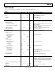
SPECIFICATIONS
VH = 3.0 V to 14.4 V
1
, VPx = 3.0 V to 6.0 V
1
, T
A
= −40°C to +85°C, unless otherwise noted.
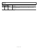
Table 1.
Parameter Min Typ Max Unit Test Conditions/Comments
POWER SUPPLY ARBITRATION
VH, VPx 3.0 V Minimum supply required on one of the VH, VPx pins
VPx 6.0 V Maximum VDDCAP = 5.1 V, typical
VH 14.4 V VDDCAP = 4.75 V
VDDCAP 2.7 4.75 5.4 V Regulated LDO output
C
VDDCAP
10 μF Minimum recommended decoupling capacitance
POWER SUPPLY
Supply Current, I
VH
, I
VPx
4.2 6 mA VDDCAP = 4.75 V, PDO1 to PDO10 off, DACs off, ADC off
Additional Currents
All PDO FET Drivers On 1 mA
VDDCAP = 4.75 V, PDO1 to PDO6 loaded with 1 μA each,
PDO7 to PDO10 off
Current Available from VDDCAP 2 mA
Maximum additional load that can be drawn from all
PDO pull-ups to VDDCAP
DAC Supply Currents 2.2 mA Six DACs on with 100 μA maximum load on each
ADC Supply Current 1 mA Running round-robin loop
EEPROM Erase Current 10 mA 1 ms duration only, VDDCAP = 3 V
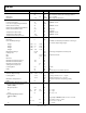
SUPPLY FAULT DETECTORS
VH Pin
Input Impedance 52 kΩ
Input Attenuator Error ±0.05 % Midrange and high range
Detection Ranges
High Range 6 14.4 V
Midrange 2.5 6 V
VPx Pins
Input Impedance 52 kΩ
Input Attenuator Error ±0.05 % Low range and midrange
Detection Ranges
Midrange 2.5 6 V
Low Range 1.25 3 V
Ultralow Range 0.573 1.375 V No input attenuation error
VXx Pins
Input Impedance 1 MΩ
Detection Range
Ultralow Range 0.573 1.375 V No input attenuation error
Absolute Accuracy ±1 %
VREF error + DAC nonlinearity + comparator offset error +
input attenuation error
Threshold Resolution 8 Bits
Digital Glitch Filter 0 μs Minimum programmable filter length
100 μs Maximum programmable filter length
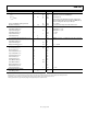
ANALOG-TO-DIGITAL CONVERTER
Signal Range 0 V
REFIN
V
The ADC can convert signals presented to the VH, VPx,
and VXx pins; VPx and VH input signals are attenuated
depending on the selected range; a signal at the pin
corresponding to the selected range is from 0.573 V to
1.375 V at the ADC input
Input Reference Voltage on REFIN Pin, V
REFIN
2.048 V
Resolution 12 Bits
INL ±2.5 LSB Endpoint corrected, V
REFIN
= 2.048 V
Gain Error ±0.05 % V
REFIN
= 2.048 V