
Datasheet

ADM1062
Rev. C | Page 9 of 36
04433-003
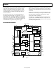
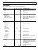
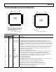
PIN CONFIGURATIONS AND FUNCTION DESCRIPTIONS
PDOGND
31
ADM1062
TOP VIEW
(Not to Scale)
GND
40
VDDCAP
39
VCCP
32
DP
38
DN
37
SDA
36
SCL
35
A1
34
A0
33
AGND
11
REFGND
12
REFIN
13
REFOUT
14
DAC1
15
DAC2
16
DAC3
17
DAC4
18
DAC5
19
DAC6
20
VX1 1
VX2
2
VX3 3
VX4 4
VX5
5
VP1
6
VP2 7
VP3 8
VP4
9
VH 10
PDO130
PDO2
29
PDO328
PDO427
PDO5
26
PDO6
25
PDO724
PDO823
PDO9
22
PDO1021
PIN 1
INDICATOR
NOTES
1. THE LFCSP HAS AN EXPOSED PAD ON THE BOTTOM.
THIS PAD IS A NO CONNECT (NC). IF POSSIBLE, THIS
PAD SHOULD BE SOLDERED TO THE BOARD FOR
IMPROVED MECHANICAL STABILITY.
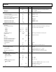
04433-004
NC = NO CONNECT
NC
48
PDOGND
38
VDDCAP
46
VCCP
39
GND
47
SDA
43
SCL
42
DN
44
NC
37
DP
45
A1
41
A0
40
Figure 3. LFCSP Pin Configuration
NC
13
AGND
14
REFGND
15
REFIN
16
REFOUT
17
DAC1
18
DAC2
19
DAC3
20
DAC4
21
DAC5
22
DAC6
23
NC
24
NC
1
NC
36
V
X1
2
V
X2
3
V
X3
4
V
X4
5
V
X5
6
V
P1
7
V
P2
8
V
P3
9
V
P4
10
VH
11
NC
12
PDO1
35
PDO2
34
PDO3
33
PDO4
32
PDO5
31
PDO6
30
PDO7
29
PDO8
28
PDO9
27
PDO10
26
NC
25
ADM1062
TOP VIEW
(Not to Scale)
PIN 1
INDICATOR
Figure 4. TQFP Pin Configuration
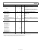
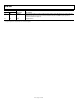
Table 4. Pin Function Descriptions
Pin No.
LFCSP
1
Mnemonic
TQFP
Description
1, 12, 13,
24, 25, 36,
37, 48
NC No Connection.
1 to 5 2 to 6 VX1 to VX5 (VXx)
High Impedance Inputs to Supply Fault Detectors. Fault thresholds can be set from 0.573 V to
1.375 V. Alternatively, these pins can be used as general-purpose digital inputs.
6 to 9 7 to 10 VP1 to VP4 (VPx)
Low Voltage Inputs to Supply Fault Detectors. Three input ranges can be set by altering the input
attenuation on a potential divider connected to these pins, the output of which connects to a supply
fault detector. These pins allow thresholds from 2.5 V to 6.0 V, from1.25 V to 3.00 V, and from 0.573 V
to 1.375 V.
10 11 VH
High Voltage Input to Supply Fault Detectors. Two input ranges can be set by altering the input
attenuation on a potential divider connected to this pin, the output of which connects to a
supply fault detector. This pin allows thresholds from 6.0 V to 14.4 V and from 2.5 V to 6.0 V.
11 14 AGND
2
Ground Return for Input Attenuators.
12 15 REFGND
2
Ground Return for On-Chip Reference Circuits.
13 16 REFIN
Reference Input for ADC. Nominally, 2.048 V. This pin must be driven by a reference voltage.
The on-board reference can be used by connecting the REFOUT pin to the REFIN pin.
14 17 REFOUT
Reference Output, 2.048 V. Typically connected to REFIN. Note that the capacitor must be
connected between this pin and REFGND. A 10 μF capacitor is recommended for this purpose.
15 to 20 18 to 23 DAC1 to DAC6
Voltage Output DACs. These pins default to high impedance at power-up.
21 to 30 26 to 35 PDO10 to PDO1
Programmable Output Drivers.
31 38 PDOGND
2
Ground Return for Output Drivers.
32 39 VCCP
Central Charge Pump Voltage of 5.25 V. A reservoir capacitor must be connected between this
pin and GND. A 10 μF capacitor is recommended for this purpose.
33 40 A0
Logic Input. This pin sets the seventh bit of the SMBus interface address.
34 41 A1
Logic Input. This pin sets the sixth bit of the SMBus interface address.
35 42 SCL
SMBus Clock Pin. Bidirectional open drain requires external resistive pull-up.
36 43 SDA
SMBus Data Pin. Bidirectional open drain requires external resistive pull-up.
37 44 DN
External Temperature Sensor Cathode Connection.
38 45 DP External Temperature Sensor Anode Connection.