
Datasheet


Super Sequencer with Margining Control
ADM1069
Rev. C
Information furnished by Analog Devices is believed to be accurate and reliable. However, no
responsibility is assumed by Analog Devices for its use, nor for any infringements of patents or other
rights of third parties that may result from its use. Specifications subject to change without notice. No
license is granted by implication or otherwise under any patent or patent rights of Analog Devices.
Trademarks and registered trademarks are the property of their respective owners.
One Technology Way, P.O. Box 9106, Norwood, MA 02062-9106, U.S.A.
Tel: 781.329.4700 www.analog.com
Fax: 781.461.3113 ©2005–2011 Analog Devices, Inc. All rights reserved.
FEATURES
Complete supervisory and sequencing solution for up to
8 supplies
8 supply fault detectors enable supervision of supplies to
<0.5% accuracy at all voltages at 25°C
<1.0% accuracy across all voltages and temperatures
4 selectable input attenuators allow supervision of supplies to
14.4 V on VH
6 V on VP1 to VP3 (VPx)
4 dual-function inputs, VX1 to VX4 (VXx)
High impedance input to supply fault detector with
thresholds between 0.573 V and 1.375 V
General-purpose logic input
8 programmable driver outputs, PDO1 to PDO8 (PDOx)
Open-collector with external pull-up
Push/pull output, driven to VDDCAP or VPx
Open-collector with weak pull-up to VDDCAP or VPx
Internally charge-pumped high drive for use with external
N-FET (PDO1 to PDO6 only)
Sequencing engine (SE) implements state machine control of
PDO outputs
State changes conditional on input events
Enables complex control of boards
Power-up and power-down sequence control
Fault event handling
Interrupt generation on warnings
Watchdog function can be integrated in SE
Program software control of sequencing through SMBus
Complete voltage margining solution for 4 voltage rails
4 voltage output 8-bit DACs (0.300 V to 1.551 V) allow voltage
adjustment via dc-to-dc converter trim/feedback node
12-bit ADC for readback of all supervised voltages
Reference input (REFIN) has 2 input options
Driven directly from 2.048 V (±0.25%) REFOUT pin
More accurate external reference for improved ADC
performance
Device powered by the highest of VPx, VH for improved
redundancy
User EEPROM: 256 bytes
Industry-standard 2-wire bus interface (SMBus)
Guaranteed PDO low with VH, VPx = 1.2 V
Available in 32-lead, 7 mm × 7 mm LQFP and 40-lead,
6 mm × 6 mm LFCSP packages
For more information about the ADM1069 register map,
refer to the AN-721 Application Note at
www.analog.com
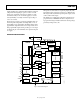
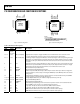
FUNCTIONAL BLOCK DIAGRAM
04735-001
PDO7
PDO8
PDOGND
VDDCA P
VDD
ARBITRATOR
DAC1
V
OUT
DAC
DAC2
V
OUT
DAC
DAC3
V
OUT
DAC
DAC4
V
OUT
DAC
GND
VCCP
VX1
VX2
VP1
VP2
VP3
VH
A
GND
PROGRAMMABLE
RESET
GENERATORS
(SFDs)
CONFIGURABLE
OUTPUT
DRIVERS
(LV CAPABLE
OF DRIVING
LOGIC SIGNALS)
PDO1
PDO2
PDO3
PDO4
PDO5
PDO6
VX3
VX4
SDA SCL A1 A0
SMBus
INTERFACE
REFIN REFOUT REFGND
VREF
12-BIT
SAR ADC
MUX
EEPROM
CLOSED-LOOP
MARGINING SYSTEM
ADM1069
DUAL-
FUNCTION
INPUTS
(LOGIC INPUTS
OR
SFDs)
SEQUENCING
ENGINE
CONFIGURABLE
OUTPUT
DRIVERS
(HV CAPABLE OF
DRIVING GATES
OF N-FET)
Figure 1.
APPLICATIONS
Central office systems
Servers/routers
Multivoltage system line cards
DSP/FPGA supply sequencing
In-circuit testing of margined supplies
GENERAL DESCRIPTION
The ADM1069 Super Sequencer® is a configurable supervisory/
sequencing device that offers a single-chip solution for supply
monitoring and sequencing in multiple supply systems. In addition
to these functions, the ADM1069 integrates a 12-bit ADC and
four 8-bit voltage output DACs. These circuits can be used to
implement a closed-loop margining system that enables supply
adjustment by altering either the feedback node or reference of
a dc-to-dc converter using the DAC outputs.