
Datasheet
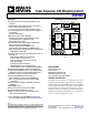


ADM1069
Rev. C | Page 7 of 32
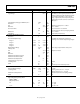
ABSOLUTE MAXIMUM RATINGS
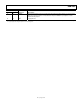
Table 2.
Parameter Rating
Voltage on VH Pin 16 V
Voltage on VPx Pins 7 V
Voltage on VXx Pins −0.3 V to +6.5 V
Voltage on A0, A1 Pins −0.3 V to +7 V
Voltage on REFIN, REFOUT Pins 5 V
Voltage on VDDCAP, VCCP Pins 6.5 V
Voltage on DACx Pins 6.5 V
Voltage on PDOx Pins 16 V
Voltage on SDA, SCL Pins 7 V
Voltage on GND, AGND, PDOGND,
REFGND Pins
−0.3 V to +0.3 V
Input Current at Any Pin ±5 mA
Package Input Current ±20 mA
Maximum Junction Temperature (T
J
max) 150°C
Storage Temperature Range −65°C to +150°C
Lead Temperature
Soldering Vapor Phase, 60 sec 215°C
ESD Rating, All Pins 2000 V
Stresses above those listed under Absolute Maximum Ratings
may cause permanent damage to the device. This is a stress
rating only; functional operation of the device at these or any
other conditions above those indicated in the operational
section of this specification is not implied. Exposure to absolute
maximum rating conditions for extended periods may affect
device reliability.
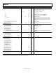
THERMAL RESISTANCE
θ
JA
is specified for the worst-case conditions, that is, a device
soldered in a circuit board for surface-mount packages.
Table 3. Thermal Resistance
Package Type θ
JA
Unit
32-Lead LQFP 54 °C/W
40-Lead LFCSP 25 °C/W
ESD CAUTION