
Datasheet


ADM1069
Rev. C | Page 9 of 32
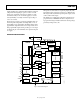
Pin No.
LQFP LFCSP
1
Mnemonic Description
31 39 VDDCAP
Device Supply Voltage. Linearly regulated from the highest of the VPx, VH pins to a typical of 4.75 V.
Note that a capacitor must be connected between this pin and GND. A 10 μF capacitor is recom-
mended for this purpose.
32 40 GND
2
Supply Ground.
1
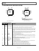
The LFCSP has an exposed pad on the bottom. This pad is a no connect (NC). If possible, this pad should be soldered to the board for improved mechanical stability.
2
In a typical application, all ground pins are connected together.