
Datasheet
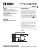

ADM1171 Data Sheet
Rev. A | Page 4 of 16
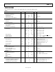
ABSOLUTE MAXIMUM RATINGS
Table 2.
Parameter Rating
V
CC
Pin −0.3 V to +20 V
SENSE Pin −0.3 V to +20 V
V
CC
− SENSE ±5 V
TIMER Pin −0.3 V to (V
CC
+ 0.3 V)
ON (ON-CLR) Pin
−0.3 V to +20 V
SS Pin –0.3 V to (V
CC
+ 0.3 V)
CSOUT Pin –0.3 V to (V
CC
+ 0.3 V)
GATE Pin −0.3 V to (V
CC
+ 11 V)
Storage Temperature Range −65°C to +125°C
Operating Temperature Range −40°C to +85°C
Lead Temperature (10 sec) 300°C
Junction Temperature 150°C
Stresses above those listed under Absolute Maximum Ratings
may cause permanent damage to the device. This is a stress
rating only; functional operation of the device at these or any
other conditions above those indicated in the operational
section of this specification is not implied. Exposure to absolute
maximum rating conditions for extended periods may affect
device reliability.
THERMAL CHARACTERISTICS
θ
JA
is specified for the worst-case conditions, that is, a device
soldered in a circuit board for surface-mount packages.
Table 3. Thermal Resistance
Package Type θ
JA
Unit
8-Lead TSOT 152.9 °C/W
ESD CAUTION
ESD (electrostatic discharge) sensitive device. Electrostatic charges as high as 4000 V readily accumulate on
the human body and test equipment and can discharge without detection. Although this product features
proprietary ESD protection circuitry, permanent damage may occur on devices subjected to high energy
electrostatic discharges. Therefore, proper ESD precautions are recommended to avoid performance
degradation or loss of functionality.