
Datasheet
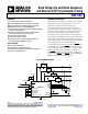

Data Sheet ADM1186
Rev. B | Page 5 of 28
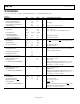
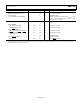
Parameter Min
Typ
Max
Unit
Test Conditions/Comments
SEQ_DONE PIN
Output Low Voltage, V
SEQ_DONEL
0.4 V V
VCC
= 2.7 V, I
SINK
= 2 mA
Leakage Current
1 µA SEQ_DONE = 5.5 V
V
VCC
That Guarantees Valid Outputs 1 V Output is guaranteed to be either low (V
SEQ_DONEL
= 0.4 V)
or giving a valid output level from V
VCC
= 1 V, I
SINK
= 30 µA
or V
VCC
= 1.1 V, I
SINK
= 100 µA
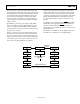
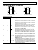
RESPONSE TIMING Includes input glitch filter and all other internal
delays
VINx to PWRGD
VINx Going Low to High 21.9 28.8 35.2 µs 50 mV input overdrive
VINx Going High to Low 5.8 7.3 8.9 µs 50 mV input overdrive
VINx to
FAULT
, OUTx Low
VINx Going High to Low (UV Fault) 6.1 7.5 9.2 µs 50 mV input overdrive
UP,
DOWN
, and UP/
DOWN
to
FAULT
,
OUTx Low, t
UDOUT
5.5 8.6 12.1 µs 100 mV input overdrive
5.8 7.7 10.5 µs 1 V input overdrive
External
FAULT
to OUTx Low 10 µs 1 V input overdrive
Fault Hold Time 35 44 54 µs U P, UP/
DOWN
held low
1
Input comparators do not include hysteresis on their inputs. The comparator output passes through a digital glitch filter to remove short transients from the input
signal that would otherwise drive the state machine.