
Datasheet
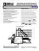

ADM1186 Data Sheet
Rev. B | Page 6 of 28
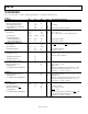
ABSOLUTE MAXIMUM RATINGS
T
A
= 25°C, unless otherwise noted.
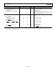
Table 2.
Parameter Rating
VCC Pin −0.3 V to +6 V
VINx Pins −0.3 V to +6 V
UP,
DOWN
, UP/
DOWN
Pins −0.3 V to +6 V
DLY_EN_OUTx, BLANK_DLY Pins −0.3 V to V
CC
+ 0.3 V
PWRGD, SEQ_DONE, OUTx Pins −0.3 V to +6 V
FAULT
Pin −0.3 V to +6 V
Operating Temperature Range −40°C to +85°C
Storage Temperature Range −65°C to +150°C
Lead Temperature Convection Reflow
Peak Temperature 260°C
Time at Peak Temperature ≤30 sec
Junction Temperature 125°C
Stresses above those listed under Absolute Maximum Ratings
may cause permanent damage to the device. This is a stress
rating only; functional operation of the device at these or any
other conditions above those indicated in the operational
section of this specification is not implied. Exposure to absolute
maximum rating conditions for extended periods may affect
device reliability.
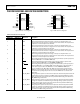
Table 3. Thermal Resistance
Package Type θ
JA
Unit
16-Lead QSOP 149.97 °C/W
20-Lead QSOP 125.80 °C/W
ESD CAUTION