
Datasheet

Data Sheet ADM1186
Rev. B | Page 7 of 28
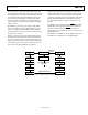
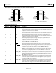
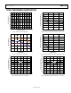
PIN CONFIGURATIONS AND FUNCTION DESCRIPTIONS
1
2
3
4
5
6
7
8
9
10
20
19
18
17
16
15
14
13
12
11
VIN1
VIN2
VIN3
DOWN
UP
VIN4
GND
OUT1
OUT2
OUT3
SEQ_DONE
PWRGD
OUT4
DLY_EN_OUT2
DLY_EN_OUT1
FAULT
DLY_EN_OUT3
DLY_EN_OUT4
BLANK_DLY
VCC
TOP VIEW
(Not to Scale)
ADM1186-1
07153-005
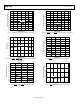
07153-006
1
2
3
4
5
6
7
8
16
15
14
13
12
11
10
9
VIN1
VIN2
VIN3
DLY_EN_OUT2
UP/DOWN
VIN4
GND
OUT1
OUT2
OUT3
BLANK_DLY
DLY_EN_OUT3 DLY_EN_OUT4
PWRGD
OUT4
VCC
TOP VIEW
(Not to Scale)
ADM1186-2
Figure 3. ADM1186-1 Pin Configuration Figure 4. ADM1186-2 Pin Configuration
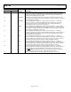
Table 4. Pin Function Descriptions
Pin No.
Mnemonic Description
ADM1186-1 ADM1186-2
1 1 GND Chip Ground Pin.
2 2 VIN1 Noninverting Comparator Input. The voltage on this pin is compared with a 0.6 V
reference. Can be used to monitor a voltage rail via a resistor divider. The output of this
comparator is monitored by the state machine.
3 3 VIN2 Noninverting Comparator Input. The voltage on this pin is compared with a 0.6 V
reference. Can be used to monitor a voltage rail via a resistor divider. The output of this
comparator is monitored by the state machine.
4 4 VIN3 Noninverting Comparator Input. The voltage on this pin is compared with a 0.6 V
reference. Can be used to monitor a voltage rail via a resistor divider. The output of this
comparator is monitored by the state machine.
5
5
VIN4
Noninverting Comparator Input. The voltage on this pin is compared with a 0.6 V
reference. Can be used to monitor a voltage rail via a resistor divider. The output of this
comparator is monitored by the state machine.
6 UP Noninverting Comparator Input. A rising edge on this pin initiates a power-up sequence
when the ADM1186-1 is in the WAIT START state.
7
DOWN
Noninverting Comparator Input. A falling edge on this pin initiates a power-down
sequence when the ADM1186-1 is in the POWER-UP DONE state.
6 UP/
DOWN
Noninverting Comparator Input. A rising edge on this pin initiates a power-up sequence
when the ADM1186-2 is in the WAIT START state. A falling edge on this pin initiates a
power-down sequence when the ADM1186-2 is in the POWER-UP DONE state.
8
FAULT
Active Low, Bidirectional, Open-Drain Pin. When an internal fault is detected by the
ADM1186-1 state machine, this pin is asserted low and the SET FAULT state is entered.
An external device pulling this pin low also causes the ADM1186-1 to enter the SET
FAULT state.
9 DLY_EN_OUT1 Timing Input. The capacitor connected to this input sets the time delay between the UP
input initiating a power-up sequence and OUT1 being asserted high. During a power-
down sequence, this input sets the time delay between OUT1 being asserted low and
SEQ_DONE being asserted low.
10 7 DLY_EN_OUT2 Timing Input. The capacitor connected to this input sets the time delay between VIN1
coming into compliance and OUT2 being asserted high during a power-up sequence.
During a power-down sequence, this input sets the time delay between OUT2 being
asserted low and OUT1 being asserted low.
11 8 DLY_EN_OUT3 Timing Input. The capacitor connected to this input sets the time delay between VIN2
coming into compliance and OUT3 being asserted high during a power-up sequence.
During a power-down sequence, this input sets the time delay between OUT3 being
asserted low and OUT2 being asserted low.