
Datasheet

Data Sheet ADM1275
Rev. D | Page 5 of 48
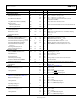
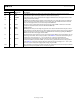
Parameter Min Typ Max Unit Test Conditions/Comments
Circuit Breaker Offset, V
CBOS
0.6 0.88 1.12 mV Circuit breaker trip voltage, V
CB
= V
SENSECL
− V
CBOS
SEVERE OVERCURRENT
Voltage Threshold, V
SENSEOC
40 50 mV V
ISET
= 1.0 V; V
FLB
> 1.1 V; V
SS
≥ 2 V
9.5 13.0 mV V
ISET
= 0.25 V; V
FLB
> 1.1 V; V
SS
≥ 2 V
Short Glitch Filter Duration 90 200 ns
V
ISET
> 1.65 V; V
SENSE
driven from 18 mV to 52 mV;
selectable via PMBus
Long Glitch Filter Duration (Default) 530 900 ns V
SENSE
driven from 18 mV to 52 mV
Response Time
With Short Glitch Filter 180 370 ns 2 mV overdrive maximum severe overcurrent threshold
With Long Glitch Filter 645 1020 ns
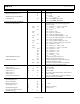
SOFT START (SS PIN)
SS Pull-Up Current, I
SS
−12 −10 −8 µA V
SS
= 0 V
Default V
SENSECL
Limit 0.5 1.25 1.8 mV
When V
SENSE
reaches this level, I
SS
is enabled, ramping
V
SENSECL
; V
SS
= 0 V
SS Pull-Down Current 100 µA V
SS
= 1 V
TIMER PIN
Timer Pull-Up Current (POR), I
TIMERUPPOR
−2 −3 −4 µA Initial power-on reset; V
TIMER
= 0.5 V
Timer Pull-Up Current (OC Fault), I
TIMERUPFLT
−57 −60 −63 µA Overcurrent fault; 0.2 V ≤ V
TIMER
≤ 1 V
Timer Pull-Down Current (Retry), I
TIMERDNRT
1.7 2 2.3 µA After fault when GATE is off; V
TIMER
= 0.5 V
Timer Retry/OC Fault Current Ratio 3.33 3.8 % Defines the limits of the autoretry duty cycle
Timer Pull-Down Current (Hold),
I
TIMERDNHOLD
100 µA Holds TIMER at 0 V when inactive; V
TIMER
= 0.5 V
Timer High Threshold, V
TIMERH
0.98 1.0 1.02 V
Timer Low Threshold, V
TIMERL
0.18 0.2 0.22 V
FOLDBACK (FLB PIN)
FLB and PWRGD Threshold, V
FLBTH
1.08 1.1 1.12 V FLB rising; V
ISET
= 1.0 V
Input Current, I
FLB
100 nA V
FLB
≤ 1.0 V; V
ISET
= 1.25 V
100 nA V
VCAP
≤ V
FLB
≤ 20 V
Hysteresis Current 1.7 2.3 μA
Internal Hysteresis Voltage 1.9 3.1 mV Voltage drop across the internal 1.3 kΩ resistor
Power-Good Glitch Filter, PWRGD
GF
0.3 0.7 1 μs 50 mV overdrive
Minimum Foldback Clamp 200 mV Accuracies included in total sense voltage accuracies
VOUT PIN ADM1275-1 and ADM1275-3
Input Current 20 μA VOUT = 20 V
LATCH PIN
ADM1275-1 and ADM1275-3
Output Low Voltage, V
OL_LATCH
0.4 V I
LATCH
= 1 mA
1.5 V I
LATCH
= 5 mA
Leakage Current 100 nA
V
LATCH
≤ 2 V; LATCH output high-Z
1
µA
V
LATCH
= 20 V; LATCH output high-Z
GPO1/ALERT1/CONV PIN (ADM1275-1 and
ADM1275-2), ENABLE PIN (ADM1275-3)
No internal pull-up present on these pins
Output Low Voltage, V
OL_GPO1
0.4 V I
GPO1
= 1 mA
1.5 V I
GPO1
= 5 mA
Leakage Current 100 nA V
GPO1
≤ 2 V; GPO output high-Z
1 µA V
GPO1
= 20 V; GPO output high-Z
Input High Voltage, V
IH
1.1 V
Input Low Voltage, V
IL
0.8
V
GPO2/ALERT2 PIN
ADM1275-1 and ADM1275-3
Output Low Voltage, V
OL_GPO2
0.4 V I
GPO2
= 1 mA
1.5
V
I
GPO2
= 5 mA
Leakage Current 100 nA V
GPO2
≤ 2 V; GPO output high-Z
1 µA V
GPO2
= 20 V; GPO output high-Z