
Datasheet

Data Sheet ADM1275
Rev. D | Page 7 of 48
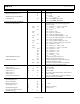
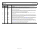
SERIAL BUS TIMING CHARACTERISTICS
t
R
= (V
IL(MAX)
– 0.15) to (V
IH3V3
+ 0.15) and t
F
= 0.9V
DD
to (V
IL(MAX)
– 0.15); where V
IH3V3
= 2.1 V and V
DD
= 3.3 V.
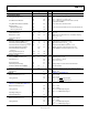
Table 2.
Parameter Description Min Typ Max Unit Test Conditions/Comments
f
SCLK
Clock frequency 400 kHz
t
BUF
Bus free time 1.3 µs Following the stop condition of a read transaction
4.7 µs Following the stop condition of a write transaction
t
HD;STA
Start hold time 0.6 µs
t
SU;STA
Start setup time 0.6 µs
t
SU;STO
Stop setup time
0.6
µs
t
HD;DAT
SDA hold time 300 900 ns
t
SU ;DAT
SDA setup time 100 ns
t
LOW
SCL low time 1.3 µs
t
HIGH
SCL high time 0.6 µs
t
R
SCL, SDA rise time 20 300 ns
t
F
SCL, SDA fall time
20
300
ns
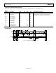
Timing Diagram
t
LOW
t
BUF
t
HD;DAT
t
SU;DAT
t
SU;STA
t
HD;STA
t
HIGH
t
R
t
F
t
SU;STO
PSSP
V
IH
V
IL
V
IH
V
IL
SCL
SDA
08931-002
Figure 2. Serial Bus Timing Diagram