
Datasheet

ADM1275 Data Sheet
Rev. D | Page 8 of 48
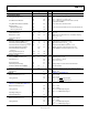
ABSOLUTE MAXIMUM RATINGS
Table 3.
Parameter Rating
VCC Pin −0.3 V to +25 V
UV Pin
−0.3 V to +4 V
OV Pin −0.3 V to +4 V
SS Pin −0.3 V to VCAP + 0.3 V
TIMER Pin −0.3 V to VCAP + 0.3 V
VCAP Pin −0.3 V to +4 V
ISET Pin −0.3 V to VCAP + 0.3 V
LATCH Pin
−0.3 V to +25 V
SCL Pin −0.3 V to +6.5 V
SDA Pin −0.3 V to +6.5 V
ADR Pin −0.3 V to VCAP + 0.3 V
GPO1/ALERT1/CONV Pin, ENABLE Pin
−0.3 V to +25 V
GPO2/ALERT2 Pin
−0.3 V to +25 V
PWRGD Pin
−0.3 V to +25 V
FLB Pin −0.3 V to +25 V
VOUT Pin −0.3 V to +25 V
GATE Pin (Internal Supply Only)
1
−0.3 V to +36 V
SENSE+ Pin −0.3 V to +25 V
SENSE− Pin
−0.3 V to +25 V
V
SENSE
(V
SENSE+
− V
SENSE−
) ±0.3 V
Continuous Current into Any Pin ±10 mA
Storage Temperature Range −65°C to +125°C
Operating Temperature Range −40°C to +85°C
Lead Temperature, Soldering (10 sec) 300°C
Junction Temperature
150°C
1
The GATE pin has internal clamping circuits to prevent the GATE pin voltage
from exceeding the maximum ratings of a MOSFET with V
GSMAX
= 20 V and
internal process limits. Applying a voltage source to this pin externally may
cause irreversible damage.
Stresses above those listed under Absolute Maximum Ratings
may cause permanent damage to the device. This is a stress
rating only; functional operation of the device at these or any
other conditions above those indicated in the operational
section of this specification is not implied. Exposure to absolute
maximum rating conditions for extended periods may affect
device reliability.
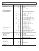
THERMAL CHARACTERISTICS
θ
JA
is specified for the worst-case conditions, that is, a device
soldered in a circuit board for surface-mount packages.
Table 4. Thermal Resistance
Package Type θ
JA
Unit
16-lead QSOP (RQ-16) 150 °C/W
20-lead QSOP (RQ-20) 126 °C/W
20-lead LFCSP (CP-20-9) 30.4 °C/W
ESD CAUTION