
Datasheet

Data Sheet ADM1275
Rev. D | Page 9 of 48
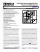
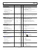
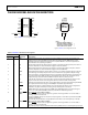
PIN CONFIGURATIONS AND FUNCTION DESCRIPTIONS
1
2
3
4
5
6
7
8
9
10
20
19
18
17
16
15
14
13
12
11
UV
OV
VCAP
TIMER
SS
ISET
VCC
SENSE–
GATE
GND
PWRGD
FLB
VOUT
GPO1/ALERT1/CONV
ADR
LATCH
GPO2/ALERT2
SDA
SCL
SENSE+
ADM1275-1
TOP VIEW
(Not to Scale)
08931-006
Figure 3. ADM1275-1 Pin Configuration, QSOP
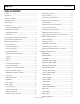
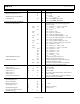
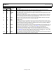
1OV
2VCAP
3ISET
4SS
5TIMER
NOTES
1. SOLDER THE EXPOSED PADDLE TO
THE BOARD TO IMPROVE THERMAL
DISSIPATION. THE EXPOSED PADDLE
CAN BE CONNECTED TO GROUND.
LATCH
ADR
GPO1/ALERT1/CONV
GPO2/ALERT2
SDA
13
14
15
12
11
FLB
VOUT
GND
PWRGD
SCL
SENSE+
VCC
UV
SENSE–
GATE
6
7
8
01
9
81
91
02
71
61
08931-109
ADM1275-1
TOP VIEW
(Not to Scale)
PIN 1
INDIC
A
TOR
Figure 4. ADM1275-1 Pin Configuration, LFCSP
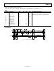
Table 5. ADM1275-1 Pin Function Descriptions
Pin No.
QSOP LFCSP Mnemonic Description
1 19 VCC
Positive Supply Input Pin. An undervoltage lockout (UVLO) circuit resets the device when a low
supply voltage is detected. GATE is held low when the supply is below UVLO. During normal
operation, this pin should remain greater than or equal to SENSE+ to ensure that specifications
are adhered to. No sequencing is required.
2 20 UV
Undervoltage Input Pin. An external resistor divider is used from the supply to this pin to allow an
internal comparator to detect whether the supply is under the UV limit.
3
1
OV
Overvoltage Input Pin. An external resistor divider is used from the supply to this pin to allow an
internal comparator to detect whether the supply is above the OV limit.
4 2 VCAP
Internal Regulated Supply. A capacitor with a value of 1 µF or greater should be placed on this pin
to maintain good accuracy. This pin can be used as a reference to program the ISET pin voltage.
5 3 ISET
This pin allows the current limit threshold to be programmed. The default limit is set when this pin
is connected directly to VCAP. To achieve a user-defined sense voltage, the current limit can be
adjusted using a resistor divider from VCAP. An external reference can also be used.
6 4 SS
Soft Start Pin. A capacitor is used on this pin to set the soft start ramp profile. The voltage on the
SS pin controls the current sense voltage limit, which controls the inrush current profile.
7 5 TIMER
Timer Pin. An external capacitor, C
TIMER
, sets an initial timing cycle delay and a fault delay. The GATE
pin is pulled low when the voltage on the TIMER pin exceeds the upper threshold.
8 6
LATCH Signals that the device is latching off after an overcurrent fault. The device can be configured for
automatic retry after latch-off by connecting this pin directly back to the UV pin.
9 7 ADR
PMBus Address Pin. This pin can be tied to GND, tied to VCAP, left floating, or tied low through a
resistor to set four different PMBus addresses (see the Device Addressing section).
10 8
GPO1/
ALERT1/
CONV
General-Purpose Digital Output (GPO1).
Alert (
ALERT1). This pin can be configured to generate an alert signal when one or more fault or
warning conditions are detected.
Conversion (CONV). This pin can be used as an input signal to control when a power monitor ADC
sampling cycle begins.
At power-up, this pin defaults to a high impedance state. There is no internal pull-up on this pin.
11 9
GPO2/
ALERT2 General-Purpose Digital Output (GPO2).
Alert (
ALERT2). This pin can be configured to generate an alert signal when one or more fault or
warning conditions are detected.
At power-up, this pin indicates the FET health mode by default. There is no internal pull-up on this pin.