
Datasheet


ADM2682E/ADM2687E
Rev. 0 | Page 18 of 24
APPLICATIONS INFORMATION
PCB LAYOUT
The ADM2682E/ADM2687E isolated RS-422/RS-485 transceiver
contains an isoPower integrated dc-to-dc converter, requiring
no external interface circuitry for the logic interfaces. Power
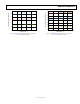
supply bypassing is required at the input and output supply pins
(see Figure 41). The power supply section of the ADM2682E/
ADM2687E uses an 180 MHz oscillator frequency to pass power
efficiently through its chip-scale transformers. In addition, the
normal operation of the data section of the iCoupler introduces
switching transients on the power supply pins.
Bypass capacitors are required for several operating frequencies.
Noise suppression requires a low inductance, high frequency
capacitor, whereas ripple suppression and proper regulation
require a large value capacitor. These capacitors are connected
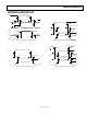
between Pin 1 (GND
1
) and Pin 2 (V
CC
) and Pin 7 (V
CC
) and
Pin 8 (GND
1
) for V
CC
. The V
ISOIN
and V
ISOOUT
capacitors are
connected between Pin 9 (GND
2
) and Pin 10 (V
ISOOUT
) and
Pin 15 (V
ISOIN
) and Pin 16 (GND
2
). To suppress noise and reduce
ripple, a parallel combination of at least two capacitors is required
with the smaller of the two capacitors located closest to the device.
The recommended capacitor values are 0.1 μF and 10 μF for
V
ISOOUT
at Pin 9 and Pin 10 and V
CC
at Pin 7 and Pin 8. Capacitor
values of 0.01 μF and 0.1 μF are recommended for V
ISOIN
at Pin 15
and Pin 16 and V
CC
at Pin 1 and Pin 2. The recommended best
practice is to use a very low inductance ceramic capacitor, or its
equivalent, for the smaller value capacitors. The total lead length
between both ends of the capacitor and the input power supply
pin should not exceed 10 mm.
09927-125
GND
1
V
CC
RxD
RE
GND
2
V
ISOIN
A
B
DE
Z
TxD
Y
V
CC
V
ISOOUT
GND
1
GND
2
1
2
3
16
15
14
4 13
5 12
6 11
7 10
8 9
ADM2682E/
ADM2687E
10n
F
10n
F
10µF 10µF
100nF 100nF
100nF 100nF
Figure 41. Recommended PCB Layout
In applications involving high common-mode transients, ensure
that board coupling across the isolation barrier is minimized.
Furthermore, design the board layout such that any coupling
that does occur equally affects all pins on a given component
side. Failure to ensure this can cause voltage differentials between
pins exceeding the absolute maximum ratings for the device,
thereby leading to latch-up and/or permanent damage.
The ADM2682E/ADM2687E dissipate approximately 675 mW
of power when fully loaded. Because it is not possible to apply
a heat sink to an isolation device, the devices primarily depend
on heat dissipation into the PCB through the GND pins. If the
devices are used at high ambient temperatures, provide a thermal
path from the GND pins to the PCB ground plane. The board
layout in Figure 41 shows enlarged pads for Pin 1, Pin 8, Pin 9,
and Pin 16. Implement multiple vias from the pad to the ground
plane to reduce the temperature inside the chip significantly. The
dimensions of the expanded pads are at the discretion of the
designer and dependent on the available board space.
EMI CONSIDERATIONS
The dc-to-dc converter section of the ADM2682E/ADM2687E
components must, of necessity, operate at very high frequency
to allow efficient power transfer through the small transformers.
This creates high frequency currents that can propagate in circuit
board ground and power planes, causing edge and dipole radiation.
Grounded enclosures are recommended for applications that
use these devices. If grounded enclosures are not possible, good
RF design practices should be followed in the layout of the PCB.
See the AN-0971 Application Note, Recommendations for
Control of Radiated Emissions with isoPower Devices, for more
information.