
Datasheet


ADM2682E/ADM2687E
Rev. 0 | Page 8 of 24
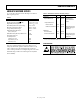
PIN CONFIGURATION AND FUNCTION DESCRIPTIONS
GND
1
1
V
CC
2
RxD
3
RE
4
GND
2
16
V
ISOIN
15
A
14
B
13
DE
5
Z
12
TxD
6
Y
11
V
CC
7
V
ISOOUT
10
GND
1
8
GND
2
9
NOTES
1. PIN 10 AND PIN 15 MUST BE
CONNECTED EXTERNALLY.
09927-002
ADM2682E/
ADM2687E
TOP VIEW
(Not to Scale)
Figure 2. Pin Configuration
Table 10. Pin Function Descriptions
Pin No. Mnemonic Description
1 GND
1
Ground, Logic Side.
2 V
CC
Logic Side Power Supply. It is recommended that a 0.1 μF and a 0.01 μF decoupling capacitor be fitted between
Pin 2 and Pin 1.
3 RxD
Receiver Output Data. This output is high when (A − B) ≥ −30 mV and low when (A − B) ≤ –200 mV. The output is
tristated when the receiver is disabled, that is, when RE
is driven high.
4
RE
Receiver Enable Input. This is an active-low input. Driving this input low enables the receiver, while driving it high
disables the receiver.
5 DE Driver Enable Input. Driving this input high enables the driver, while driving it low disables the driver.
6 TxD Driver Input. Data to be transmitted by the driver is applied to this input.
7 V
CC
Logic Side Power Supply. It is recommended that a 0.1 μF and a 10 μF decoupling capacitor be fitted between
Pin 7 and Pin 8.
8 GND
1
Ground, Logic Side.
9 GND
2
Ground, Bus Side.
10 V
ISOOUT
Isolated Power Supply Output. This pin must be connected externally to V
ISOIN
. It is recommended that a reservoir
capacitor of 10 μF and a decoupling capacitor of 0.1 μF be fitted between Pin 10 and Pin 9.
11 Y Driver Noninverting Output
12 Z Driver Inverting Output
13 B Receiver Inverting Input.
14 A Receiver Noninverting Input.
15 V
ISOIN
Isolated Power Supply Input. This pin must be connected externally to V
ISOOUT
. It is recommended that a 0.1 μF
and a 0.01 μF decoupling capacitor be fitted between Pin 15 and Pin 16.
16 GND
2
Ground, Bus Side.