
Datasheet

Data Sheet ADM6316/ADM6317/ADM6318/ADM6319/ADM6320/ADM6321/ADM6322
Rev. F | Page 9 of 16
CIRCUIT DESCRIPTION
The ADM6316/ADM6317/ADM6318/ADM6319/ADM6320/
ADM6321/ADM6322 provide microprocessor supply voltage
supervision by controlling the microprocessor’s reset input. Code
execution errors are avoided during power-up, power-down,
and brownout conditions by asserting a reset signal when the
supply voltage is below a preset threshold and by allowing
supply voltage stabilization with a fixed timeout reset pulse
after the supply voltage rises above the threshold. In addition,
problems with microprocessor code execution can be monitored
and corrected with a watchdog timer (ADM6316/ADM6317/
ADM6318/ADM6320/ADM6321). If the user detects a problem
with the system’s operation, a manual reset input is available
(ADM6316/ADM6317/ADM6319/ADM6320/ADM6322) to
reset the microprocessor, for example, by means of an external
push button.
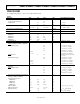
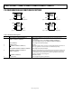
RESET OUTPUT
The ADM6316 features an active-low push-pull reset output,
while the ADM6317/ADM6321/ADM6322 have active-high
push-pull reset outputs. The ADM6318/ADM6319 feature dual
active-low and active-high push-pull reset outputs. For active-
low and active-high outputs, the reset signal is guaranteed to be
logic low and logic high, respectively, for V
CC
down to 1 V.
The reset output is asserted when V
CC
is below the reset thresh-
old (V
TH
), when
MR
is driven low, or when WDI is not serviced
within the watchdog timeout period (t
WD
). Reset remains asserted
for the duration of the reset active timeout period (t
RP
) after V
CC
rises above the reset threshold, after
MR
transitions from low to
high, or after the watchdog timer times out. Figure 17 illustrates
the behavior of the reset outputs.
V
CC
1V
V
CC
0V
V
CC
0V
V
TH
V
TH
0V
V
CC
RESET
RESET
t
RD
t
RD
1V
t
RP
t
RP
04533-019
Figure 17. Reset Timing Diagram
OPEN-DRAIN RESET OUTPUT
The ADM6320/ADM6321/ADM6322 have an active-low, open-
drain reset output. This output structure requires an external
pull-up resistor to connect the reset output to a voltage rail no
higher than 6 V. The resistor should comply with the micro-
processor’s logic low and logic high voltage level requirements
while supplying input current and leakage paths on the
RESET
line. A 10 kΩ resistor is adequate in most situations.
MANUAL RESET INPUT
The ADM6316/ADM6317/ADM6319/ADM6320/ADM6322
feature a manual reset input (
MR
), which when driven low, asserts
the reset output. When
MR
transitions from low to high, reset
remains asserted for the duration of the reset active timeout
period before deasserting. The
MR
input has a 52 kΩ, internal
pull-up so that the input is always high when unconnected. An
external push-button switch can be connected between
MR
and
ground so that the user can generate a reset. Debounce circuitry
for this purpose is integrated on chip. Noise immunity is provided
on the
MR
input, and fast, negative-going transients of up to
100 ns (typical) are ignored. A 0.1 μF capacitor between
MR
and
ground provides additional noise immunity.
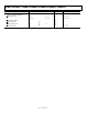
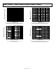
WATCHDOG INPUT
The ADM6316/ADM6317/ADM6318/ADM6320/ADM6321
feature a watchdog timer that monitors microprocessor activity.
A timer circuit is cleared with every low-to-high or high-to-low
logic transition on the watchdog input pin (WDI), which detects
pulses as short as 50 ns. If the timer counts through the preset
watchdog timeout period (t
WD
), reset is asserted. The micro-
processor is required to toggle the WDI pin to avoid being reset.
Failure of the microprocessor to toggle WDI within the timeout
period, therefore, indicates a code execution error, and the reset
pulse generated restarts the microprocessor in a known state.
As well as logic transitions on WDI, the watchdog timer is also
cleared by a reset assertion due to an undervoltage condition on
V
CC
or due to
MR
being pulled low. When reset is asserted, the
watchdog timer is cleared and does not begin counting again
until reset deassserts. The watchdog timer can be disabled by
leaving WDI floating or by three-stating the WDI driver.
V
CC
1V
V
CC
0V
V
CC
0V
V
TH
0V
V
CC
WDI
RESET
t
RP
t
RP
t
WD
04533-022
Figure 18. Watchdog Timing Diagram