
Datasheet
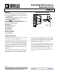
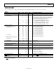

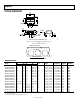
Table Of Contents

ADM6339
Rev. A | Page 3 of 12
SPECIFICATIONS
V
IN2
= 1.0 V to 5.5 V, T
A
= −40°C to +85°C, unless otherwise noted. Typical values are V
IN2
= 3.0 V to 3.3 V, T
A
= 25°C.
Table 1.
Parameter Min Typ Max Units Test Conditions/Comments
OPERATING VOLTAGE RANGE (V
IN2
)
1, 2
1.0
5.5 V
INPUT CURRENT
IN
x
Input Current
25 40 μA V
INx
= nominal input voltage for 1.8 V, 2.5 V, and 5.0 V supplies.
55 115 μA V
IN2
= nominal input voltage for 3.0 V and 3.3 V supplies. V
IN2
is
also the device power supply. The supply splits into 25 μA for
the resistor divider and 30 μA for other circuits.
−0.1 +0.1 μA V
INx
= 0 V to V
IN2
(input threshold voltage = 1.23 V).
0.4 1.5 μA V
IN1
= 1.5 V (ADM6339K and ADM6639L models only).
−15 −20 μA V
INx
= −5.0 V (IN
x
input threshold voltage = −5.0 V).
−0.1 +0.1 μA V
INx
= 0.62 V (IN
x
input threshold voltage = 0.62 V).
−1 −3 −5 μA V
INx
= −0.5 V (IN
x
input threshold voltage = −0.5 V).
THRESHOLD VOLTAGE
Fixed Threshold Voltage (V
TH
) 4.50 4.63 4.75 V 5.0 V (−5% tolerance) threshold.
V
INx
Decreasing 4.25 4.38 4.50 V 5.0 V (−10% tolerance) threshold.
3.00 3.08 3.15 V 3.3 V (−5% tolerance) threshold.
2.85 2.93 3.00 V 3.3 V (−10% tolerance) threshold.
2.70 2.78 2.85 V 3.0 V (−5% tolerance) threshold.
2.55 2.63 2.70 V 3.0 V (−10% tolerance) threshold.
2.13 2.19 2.25 V 2.5 V (−10% tolerance) threshold.
1.53 1.58 1.62 V 1.8 V (−10% tolerance) threshold.
V
INx
Increasing −4.75 −4.63 −4.50 V −5.0 V (+5% tolerance) threshold.
−4.50 −4.38 −4.25 V −5.0 V (+10% tolerance) threshold.
Adjustable Threshold Voltage (V
TH
)
V
INx
Decreasing 1.20 1.23 1.26 V
0.615 0.620 0.625 V
V
INx
Increasing −0.497 −0.487 −0.477 V −0.5 V threshold.
RESET THRESHOLD HYSTERESIS (V
HYST
) 0.3 % V
TH
0.47 % V
TH
IN
4
, ADM6339Q model.
RESET THRESHOLD TEMPERATURE
COEFFICIENT (TCV
TH
)
60 ppm/°C
IN
X
to RESET DELAY (t
RD
) 30 μs V
INx
= V
TH
to (V
TH
− 50 mV) for all inputs except −0.5 V and −5.0 V;
V
INx
= V
TH
to (V
TH
+ 50 mV) for −5.0 V and −0.5 V inputs only.
RESET TIMEOUT PERIOD (t
RP
) 140 200 280 ms
RESET
OUTPUT LOW (V
OL
)
0.4 V V
IN2
= 5.0 V, I
SINK
= 2 mA.
0.4 V V
IN2
= 2.5 V, I
SINK
= 1.2 mA.
0.4 V V
IN2
= V
IN1
= 1 V, I
SINK
= 50 μA.
0.4 V V
IN1
=1V, V
IN2
= 0 V, I
SINK
= 20 μA
0.4 V V
IN1
=0 V, V
IN2
= 1 V, I
SINK
= 20 μA
RESET
OUTPUT HIGH (V
OH
)
0.8 × V
IN2
V
V
IN2
≥ 2.55 V, I
SOURCE
= 6 μA,
RESET
not asserted.
RESET
OUTPUT HIGH SOURCE
CURRENT (I
OH
)
10 μA
V
IN2
≥ 2.55 V,
RESET
not asserted.
1
The device is powered by Input IN
2
.
2
The
RESET
output is guaranteed to be in the correct state for IN
1
or IN
2
down to 1 V.