
Datasheet


ADM6711/ADM6713 Data Sheet
Rev. B | Page 6 of 12
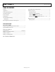
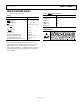
PIN CONFIGURATION AND FUNCTION DESCRIPTIONS
GND
1
RESET
2
V
CC
4
MR
3
ADM6711/
ADM6713
TOP VIEW
(Not to Scale)
03754-003
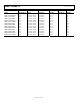
Figure 4. Pin Configuration
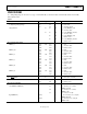
Table 4. Pin Function Descriptions
Pin No. Mnemonic Description
1 GND Ground Reference for All Signals (0 V).
2
RESET
Active Low Logic Input. RESET remains low while V
CC
is below the reset threshold and remains low for
240 ms (typical) after V
CC
rises above the reset threshold.
3
MR
Manual Reset. This active low debounced input ignores input pulses of 100 ns (typical) and is guaranteed
to accept input pulses greater than 1 µs. Leave floating when not used.
4 V
CC
Supply Voltage Being Monitored.