
Datasheet
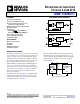


ADM6711/ADM6713 Data Sheet
Rev. B | Page 8 of 12
CIRCUIT DESCRIPTION
The ADM6711/ADM6713 are designed to protect the integrity
of a system’s operation by ensuring the proper operation of the
system during power-up, power-down, and brownout conditions.
When the ADM6711/ADM6713 are powered up, the
RESET
output remains low for a period equal to the typical reset active
timeout period. This is designed to give the system time to power
up correctly and for the power supply to stabilize before any
devices are brought out of reset and allowed to begin executing
instructions. Initializing a system in this way provides a more
reliable startup for microprocessor systems.
MANUAL RESET INPUT
The ADM6711/ADM6713 manual reset (
MR
) input allows the
system operator to reset a system by means of an external manual
switch. Alternatively, a logic signal from another digital circuit
can be used to trigger a reset via the
MR
input.
The
MR
input ignores negative-going pulses faster than 100 ns
(typical) and is guaranteed to accept any negative-going input
pulse of a duration greater than or equal to 1 μs. The
RESET
output remains low while
MR
is held low and for 240 ms
(typical) after
MR
returns high.
If
MR
is connected to long cables or is used in a noisy environment,
then placing a 0.1 μF capacitor between the
MR
input and ground
helps to remove any fast, negative-going transients.
POWER SUPPLY GLITCH IMMUNITY
The ADM6711/ADM6713 contain internal filtering circuitry
that provides immunity to fast transient glitches on the power
supply line. Figure 9 illustrates glitch immunity performance by
showing the maximum transient duration without causing a reset
pulse for glitches with amplitudes in the range of 1 mV to 1000 mV.
Glitch immunity makes the ADM6711/ADM6713 suitable for
use in noisy environments. Mounting a 0.1 μF decoupling
capacitor as close as possible to the V
CC
pin improves glitch
immunity further.
ADM6713
RESET
OUTPUT LOGIC LEVELS
The ADM6713 open-drain
RESET
output is designed for use with
an external pull-up resistor. This resistor can be tied to V
CC
or
any other reasonable voltage level, offering the flexibility to use
the to drive a variety of different logic level circuitry. ADM6713
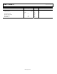
ENSURING A VALID
RESET
OUTPUT DOWN TO
V
CC
= 0 V
When V
CC
falls below 0.8 V, the ADM6711/ADM6713
RESET
output no longer sinks current, and a high impedance CMOS
logic input connected to
RESET
may drift to undetermined
logic levels. To eliminate this problem, a pull-down resistor is
connected from
RESET
to ground. A 100 kΩ resistor is large enough
not to load
RESET
and small enough to pull
RESET
to ground.
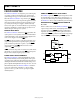
RESET
GND
ADM6711
100kΩ
03754-010
V
CC
V
CC
ADM6711
V
CC
GND
RESET
RESET
GENERATOR
240ms
DEBOUNCE
MR
V
REF
0
3754-011
Figure 10. Ensuring a Valid
RESET
Output Down to V
CC
= 0 V