
Datasheet
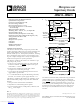
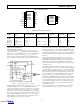


REV. A
Information furnished by Analog Devices is believed to be accurate and
reliable. However, no responsibility is assumed by Analog Devices for its
use, nor for any infringements of patents or other rights of third parties
which may result from its use. No license is granted by implication or
otherwise under any patent or patent rights of Analog Devices.
a
Microprocessor
Supervisory Circuits
ADM690–ADM695
FEATURES
Superior Upgrade for MAX690–MAX695
Specified Over Temperature
Low Power Consumption (5 mW)
Precision Voltage Monitor
Reset Assertion Down to 1 V V
CC
Low Switch On-Resistance 1.5 V Normal,
20 V in Backup
High Current Drive (100 mA)
Watchdog Timer—100 ms, 1.6 s, or Adjustable
600 nA Standby Current
Automatic Battery Backup Power Switching
Extremely Fast Gating of Chip Enable Signals (5 ns)
Voltage Monitor for Power Fail
APPLICATIONS
Microprocessor Systems
Computers
Controllers
Intelligent Instruments
Automotive Systems
GENERAL DESCRIPTION
The ADM690–ADM695 family of supervisory circuits offers
complete single chip solutions for power supply monitoring and
battery control functions in microprocessor systems. These
functions include µP reset, backup battery switchover, watchdog
timer, CMOS RAM write protection, and power failure warn-
ing. The complete family provides a variety of configurations to
satisfy most microprocessor system requirements.
The ADM690, ADM692 and ADM694 are available in 8-pin
DIP packages and provide:
1. Power-on reset output during power-up, power-down and
brownout conditions. The
RESET output remains opera-
tional with V
CC
as low as 1 V.
2. Battery backup switching for CMOS RAM, CMOS
microprocessor or other low power logic.
3. A reset pulse if the optional watchdog timer has not been
toggled within a specified time.
4. A 1.3 V threshold detector for power fail warning, low battery
detection, or to monitor a power supply other than +5 V.
The ADM691, ADM693 and ADM695 are available in 16-pin
DIP and small outline packages and provide three additional
functions.
1. Write protection of CMOS RAM or EEPROM.
2. Adjustable reset and watchdog timeout periods.
3. Separate watchdog timeout, backup battery switchover, and
low V
CC
status outputs.
The ADM690–ADM695 family is fabricated using an advanced
epitaxial CMOS process combining low power consumption
(5 mW), extremely fast Chip Enable gating (5 ns) and high reli-
ability.
RESET assertion is guaranteed with V
CC
as low as 1 V.
In addition, the power switching circuitry is designed for mini-
mal voltage drop thereby permitting increased output current
drive of up to 100 mA without the need for an external pass
transistor.
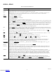
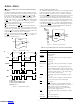
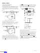
FUNCTIONAL BLOCK DIAGRAMS
4.65V
1
WATCHDOG
TRANSITION DETECTOR
1.3V
ADM691
ADM693
ADM695
V
OUT
V
BATT
V
CC
WATCHDOG
INPUT (WDI)
POWER FAIL
INPUT (PFI)
1
VOLTAGE DETECTOR = 4.65V (ADM691, ADM695)
4.40V (ADM693)
POWER FAIL
OUTPUT (PFO)
RESET
WATCHDOG
TIMER
RESET &
WATCHDOG
TIMEBASE
RESET
GENERATOR
BATT ON
OSC IN
OSC SEL
WATCHDOG
OUTPUT (WDO)
RESET
LOW LINE
CE
OUT
CE
IN
4.65V
1
RESET
GENERATOR
2
WATCHDOG
TRANSITION DETECTOR
(1.6s)
1.3V
ADM690
ADM692
ADM694
V
OUT
V
BATT
V
CC
WATCHDOG
INPUT (WDI)
POWER FAIL
INPUT (PFI)
1
VOLTAGE DETECTOR = 4.65V (ADM690, ADM694)
4.40V (ADM692)
2
RESET PULSE WIDTH = 50ms (ADM690, ADM692)
200ms (ADM694)
POWER FAIL
OUTPUT (PFO)
RESET
© Analog Devices, Inc., 1996
One Technology Way, P.O. Box 9106, Norwood, MA 02062-9106, U.S.A.
Tel: 617/329-4700 Fax: 617/326-8703
Downloaded from Arrow.com.