
Datasheet


ADM690–ADM695
REV. A
–12–
ADM690
ADM692
ADM694
R
2
R
1
PFO
+5V
V
CC
CMOS RAM
POWER
I/O LINE
µP NMI
µP RESET
µP SYSTEM
µP POWER
V
OUT
RESET
WDI
GND
PFI
V
BATT
BATTERY
+
0.1µF
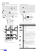
Figure 23a. ADM690/ADM692/ADM694 Typical Application
Circuit A
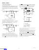
Figure 23b shows a similar application but in this case the PFI
input monitors the unregulated input to the 7805 voltage regu-
lator. This gives an earlier warning of an impending power fail-
ure. It is useful with processors operating at low speeds or
where there are a significant number of housekeeping tasks to be
completed before the power is lost.
ADM690
ADM692
ADM694
R
2
R
1
PFO
7805
INPUT
POWER
V > 8V
+5V
V
CC
CMOS RAM
POWER
I/O LINE
µP NMI
µP RESET
µP SYSTEM
µP POWER
V
OUT
RESET
WDI
GND
PFI
V
BATT
0.1µF
BATTERY
0.1µF
Figure 23b. ADM690/ADM692/ADM694 Typical Application
Circuit B
ADM691, ADM693, ADM695
A typical connection for the ADM691/ADM693/ADM695 is
shown in Figure 24. CMOS RAM is powered from V
OUT
. When
5 V power is present this is routed to V
OUT
. If V
CC
fails then
V
BATT
is routed to V
OUT
. V
OUT
can supply up to 100 mA from
V
CC
, but if more current is required, an external PNP transistor
can be added. When V
CC
is higher than V
BATT
, the BATT ON
output goes low, providing up to 25 mA of base drive for the
external transistor. A 0.1 µF capacitor is connected to V
OUT
to
supply the transient currents for CMOS RAM. When V
CC
is
lower than V
BATT
, an internal 20 Ω MOSFET connects the
backup battery to V
OUT
.
R =(V
CC
– 50 mV)/1 µA
Note that the resistor will discharge the battery slightly. With a
V
CC
supply of 4.5 V, a suitable resistor is 4.3 MΩ. With a 3 V
battery this will draw around 700 nA. This will be negligible in
most cases.
ADM69x
V
BATT
BATTERY
R
Figure 22b. Preventing Spurious RESETS During Battery
Replacement
TYPICAL APPLICATIONS
ADM690, ADM692 AND ADM694
Figure 23 shows the ADM690/ADM692/ADM694 in a typical
power monitoring, battery backup application. V
OUT
powers the
CMOS RAM. Under normal operating conditions with V
CC
present, V
OUT
is internally connected to V
CC
. If a power failure
occurs, V
CC
will decay and V
OUT
will be switched to V
BATT
thereby maintaining power for the CMOS RAM. A RESET
pulse is also generated when V
CC
falls below 4.65 V for the
ADM690/ADM694 or 4.4 V for the ADM692.
RESET will
remain low for 50 ms (200 ms for ADM694) after V
CC
returns
to 5 V.
The watchdog timer input (WDI) monitors an I/O line from the
µP system. This line must be toggled once every 1.6 seconds to
verify correct software execution. Failure to toggle the line indi-
cates that the µP system is not correctly executing its program
and may be tied up in an endless loop. If this happens, a reset
pulse is generated to initialize the processor.
If the watchdog timer is not needed, the WDI input should be
left floating.
The Power Fail Input, PFI, monitors the input power supply via
a resistive divider network. The voltage on the PFI input is com-
pared with a precision 1.3 V internal reference. If the input volt-
age drops below 1.3 V, a power fail output (
PFO) signal is
generated. This warns of an impending power failure and may
be used to interrupt the processor so that the system may be
shut down in an orderly fashion. The resistors in the sensing
network are ratioed to give the desired power fail threshold
voltage V
T
.
V
T
= (1.3 R
1
/R
2
) + 1.3 V
R
1
/R
2
= (V
T
/1.3) – 1
Downloaded from Arrow.com.Downloaded from Arrow.com.Downloaded from Arrow.com.Downloaded from Arrow.com.Downloaded from Arrow.com.Downloaded from Arrow.com.Downloaded from Arrow.com.Downloaded from Arrow.com.Downloaded from Arrow.com.Downloaded from Arrow.com.Downloaded from Arrow.com.Downloaded from Arrow.com.