
Datasheet


ADM690–ADM695
REV. A
–13–
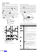
ADM691
ADM693
ADM695
R
2
R
1
PFO
INPUT POWER
+5V
V
CC
V
OUT
WDI
GND
PFI
V
BATT
0.1µF
3V
BATTERY
RESET
0.1µF
OSC IN
OSC SEL
LOW LINE WDO
SYSTEM STATUS
INDICATORS
CMOS
RAM
ADDRESS
DECODE
I/O LINE
NMI
RESET
A0–A15
µP
0.1µF
RESET
CE
OUT
CE
IN
BATT
ON
NC
Figure 24. ADM691/ADM693/ADM695 Typical Application
Reset Output
The internal voltage detector monitors V
CC
and generates a
RESET output to hold the microprocessor’s Reset line low
when V
CC
is below 4.65 V (4.4 V for ADM693). An internal
timer holds
RESET low for 50 ms (200 ms for the ADM695)
after V
CC
rises above 4.65 V (4.4 V for ADM693). This prevents
repeated toggling of
RESET even if the 5 V power drops out
and recovers with each power line cycle.
The crystal oscillator normally used to generate the clock for mi-
croprocessors can take several milliseconds to stabilize. Since
most microprocessors need several clock cycles to reset,
RESET
must be held low until the microprocessor clock oscillator has
started. The power-up
RESET pulse lasts 50 ms (200 ms for the
ADM695) to allow for this oscillator start-up time. If a different
reset pulse width is required, then a capacitor should be con-
nected to OSC IN or an external clock may be used. Please refer
to Table I and Figure 4. The manual reset switch and the 0.1 µF
capacitor connected to the reset line can be omitted if a manual
reset is not needed. An inverted, active high, RESET output is
also available.
Power Fail Detector
The +5 V V
CC
power line is monitored via a resistive potential
divider connected to the Power Fail Input (PFI). When the
voltage at PFI falls below 1.3 V, the Power Fail Output (
PFO)
drives the processor’s NMI input low. If for example a Power
Fail threshold of 4.8 V is set with resistors R
1
and R
2
, the micro-
processor will have the time when V
CC
falls from 4.8 V to 4.65 V
to save data into RAM. An earlier power fail warning can be
generated if the unregulated dc input to the 5 V regulator is
available for monitoring. This will allow more time for micro-
processor housekeeping tasks to be completed before power is
lost.
RAM Write Protection
The ADM691/ADM693/ADM695 CE
OUT
line drives the Chip
Select inputs of the CMOS RAM.
CE
OUT
follows CE
IN
as long
as V
CC
is above the 4.65 V (4.4 V for ADM693) reset threshold.
If V
CC
falls below the reset threshold, CE
OUT
goes high, inde-
pendent of the logic level at
CE
IN
. This prevents the micropro-
cessor from writing erroneous data into RAM during power-up,
power-down, brownouts and momentary power interruptions.
Watchdog Timer
The microprocessor drives the Watchdog Input (WDI) with an
I/O line. When OSC IN and OSC SEL are unconnected, the
microprocessor must toggle the WDI pin once every 1.6 sec-
onds to verify proper software execution. If a hardware or soft-
ware failure occurs such that WDI not toggled, the ADM691/
ADM693 will issue a 50 ms (200 ms for ADM695)
RESET
pulse after 1.6 seconds. This typically restarts the micro-
processor’s power-up routine. A new
RESET pulse is issued
every 1.6 seconds until WDI is again strobed. If a different
watchdog timeout period is required, then a capacitor should be
connected to OSC IN or an external clock may be used. Please
refer to Table I and Figure 4.
The WATCHDOG OUTPUT (
WDO) goes low if the watch-
dog timer is not serviced within its timeout period. Once
WDO
goes low, it remains low until a transition occurs at WDI. The
watchdog timer feature can be disabled by leaving WDI
unconnected.
The
RESET output has an internal 3 µA pull-up, and can either
connect to an open collector reset bus or directly drive a CMOS
gate without an external pull-up resistor.
Downloaded from Arrow.com.Downloaded from Arrow.com.Downloaded from Arrow.com.Downloaded from Arrow.com.Downloaded from Arrow.com.Downloaded from Arrow.com.Downloaded from Arrow.com.Downloaded from Arrow.com.Downloaded from Arrow.com.Downloaded from Arrow.com.Downloaded from Arrow.com.Downloaded from Arrow.com.Downloaded from Arrow.com.