
Datasheet
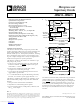


ADM690–ADM695
REV. A
–4–
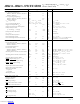
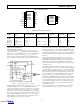
PIN FUNCTION DESCRIPTION
Mnemonic Function
V
CC
Power Supply Input: +5 V Nominal.
V
BATT
Backup Battery Input. Connect to Ground if a backup battery is not used.
V
OUT
Output Voltage, V
CC
or V
BATT
is internally switched to V
OUT
depending on which is at the highest potential. V
OUT
can supply up to 100 mA to power CMOS RAM. Connect V
OUT
to V
CC
if V
OUT
and V
BATT
are not used.
GND 0 V. Ground reference for all signals.
RESET Logic Output. RESET goes low if
1. V
CC
falls below the Reset Threshold
2. V
CC
falls below V
BATT
3. The watchdog timer is not serviced within its timeout period.
The reset threshold is typically 4.65 V for the ADM690/ADM691/ADM694/ADM695 and 4.4 V for the ADM692 and
ADM693.
RESET remains low for 50 ms (ADM690/ADM691/ADM692/ADM693) or 200 ms (ADM694/ADM695)
after V
CC
returns above the threshold. RESET also goes low for 50 (200) ms if the watchdog timer is enabled but not
serviced within its timeout period. The
RESET pulse width can be adjusted on the ADM691/ADM693/ADM695 as
shown in Table I. The
RESET output has an internal 3 µA pull up, and can either connect to an open collector
Reset bus or directly drive a CMOS gate without an external pull-up resistor.
WDI Watchdog Input. WDI is a three level input. If WDI remains either high or low for longer than the watchdog timeout
period,
RESET pulses low and WDO goes low. The timer resets with each transition on the WDI line. The watchdog
timer may be disabled if WDI is left floating or is driven to midsupply.
PFI Power Fail Input. PFI is the noninverting input to the Power Fail Comparator when PFI is less than 1.3 V,
PFO
goes low. Connect PFI to GND or V
OUT
when not used.
PFO Power Fail Output. PFO is the output of the Power Fail Comparator. It goes low when PFI is less than 1.3 V. The
comparator is turned off and
PFO goes low when V
CC
is below V
BATT
.
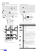
CE
IN
Logic Input. The input to the CE gating circuit. Connect to GND or V
OUT
if not used.
CE
OUT
Logic Output. CE
OUT
is a gated version of the CE
IN
signal. CE
OUT
tracks CE
IN
when V
CC
is above the reset
threshold. If V
CC
is below the reset threshold, CE
OUT
is forced high. See Figures 5 and 6.
BATT ON Logic Output. BATT ON goes high when V
OUT
is internally switched to the V
BATT
input. It goes low when V
OUT
is internally switched to V
CC
. The output typically sinks 35 mA and can directly drive the base of an external
PNP transistor to increase the output current above the 100 mA rating of V
OUT
.
LOW LINE Logic Output. LOW LINE goes low when V
CC
falls below the reset threshold. It returns high as soon as V
CC
rises
above the reset threshold.
RESET Logic Output. RESET is an active high output. It is the inverse of
RESET.
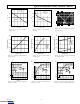
OSC SEL Logic Oscillator Select Input. When OSC SEL is unconnected (floating) or driven high, the internal oscillator sets
the reset active time and watchdog timeout period. When OSC SEL is low, the external oscillator input, OSC IN,
is enabled. OSC SEL has a 3 µA internal pull up, (see Table I).
OSC IN Oscillator Logic Input. With OSC SEL low, OSC IN can be driven by an external clock signal or an external
capacitor can be connected between OSC IN and GND. This sets both the reset active pulse timing and the watch-
dog timeout period (see Table I and Figure 4). With OSC SEL high or floating, the internal oscillator is enabled
and the reset active time is fixed at 50 ms typ. (ADM691/ADM693) or 200 ms typ (ADM695). In this mode the
OSC IN pin selects between fast (100 ms) and slow (1.6 s) watchdog timeout periods. In both modes, the timeout
period immediately after a reset is 1.6 s typical.
WDO Logic Output. The Watchdog Output, WDO, goes low if WDI remains either high or low for longer than the
watchdog timeout period.
WDO is set high by the next transition at WDI. If WDI is unconnected or at midsupply,
the watchdog timer is disabled and WDO remains high. WDO also goes high when LOW LINE goes low.
Downloaded from Arrow.com.Downloaded from Arrow.com.Downloaded from Arrow.com.Downloaded from Arrow.com.