
Datasheet


ADM690–ADM695
REV. A
–5–
PIN CONFIGURATIONS
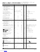
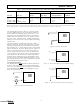
PRODUCT SELECTION GUIDE
Part Nominal Reset Nominal V
CC
Nominal Watchdog Battery Backup Base Drive Chip Enable
Number Time Reset Threshold Timeout Period Switching Ext PNP Signals
ADM690 50 ms 4.65 V 1.6 s Yes No No
ADM691 50 ms or ADJ 4.65 V 100 ms, 1.6 s, ADJ Yes Yes Yes
ADM692 50 ms 4.4 V 1.6 s Yes No No
ADM693 50 ms or ADJ 4.4 V 100 ms, 1.6 s, ADJ Yes Yes Yes
ADM694 200 ms 4.65 V 1.6 s Yes No No
ADM695 200 ms or ADJ 4.65 V 100 ms, 1.6 s, ADJ Yes Yes Yes
CIRCUIT INFORMATION
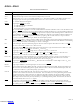
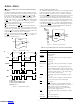
Battery Switchover Section
The battery switchover circuit compares V
CC
to the V
BATT
input, and connects V
OUT
to whichever is higher. Switchover
occurs when V
CC
is 50 mV higher than V
BATT
as V
CC
falls, and
when V
CC
is 70 mV greater than V
BATT
as V
CC
rises. This
20 mV of hysteresis prevents repeated rapid switching if V
CC
falls very slowly or remains nearly equal to the battery voltage.
Figure 1. Battery Switchover Schematic
During normal operation with V
CC
higher than V
BATT
, V
CC
is in-
ternally switched to V
OUT
via an internal PMOS transistor
switch. This switch has a typical on-resistance of 1.5 Ω and can
supply up to 100 mA at the V
OUT
terminal. V
OUT
is normally
used to drive a RAM memory bank which may require instanta-
neous currents of greater than 100 mA. If this is the case then a
bypass capacitor should be connected to V
OUT
. The capacitor
will provide the peak current transients to the RAM. A capaci-
tance value of 0.1 µF or greater may be used.
If the continuous output current requirement at V
OUT
exceeds
100 mA or if a lower V
CC
–V
OUT
voltage differential is desired,
an external PNP pass transistor may be connected in parallel
with the internal transistor. The BATT ON output (ADM691/
ADM693/ADM695) can directly drive the base of the external
transistor.
A 20 Ω MOSFET switch connects the V
BATT
input to V
OUT
during battery backup. This MOSFET has very low input-to-
output differential (dropout voltage) at the low current levels
required for battery back up of CMOS RAM or other low
power CMOS circuitry. The supply current in battery back up
is typically 0.6 µA.
The ADM690/ADM691/ADM694/ADM695 operates with
battery voltages from 2.0 V to 4.25 V and the ADM692/ADM693
operates with battery voltages from 2.0 V to 4.0 V. High value
capacitors, either standard electrolytic or the farad size double
layer capacitors, can also be used for short-term memory back
up. A small charging current of typically 10 nA (0.1 µA max)
flows out of the V
BATT
terminal. This current is useful for
maintaining rechargeable batteries in a fully charged condition.
This extends the life of the back up battery by compensating
for its self discharge current. Also note that this current poses
no problem when lithium batteries are used for back up since
the maximum charging current (0.1 µA) is safe for even the
smallest lithium cells.
If the battery-switchover section is not used, V
BATT
should be
connected to GND and V
OUT
should be connected to V
CC
.
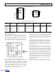
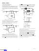
1
2
3
4
5
6
7
8
16
15
14
13
12
11
10
9
TOP VIEW
(Not to Scale)
ADM691
ADM693
ADM695
GND
V
BATT
V
OUT
PFI
PFO
WDO
V
CC
RESET
BATT ON
LOW LINE
OSC IN
OSC SEL
RESET
CE
IN
CE
OUT
WDI
GND
V
BATT
V
OUT
PFI
PFO
WDI
RESET
V
CC
1
2
3
4
8
7
6
5
TOP VIEW
(Not to Scale)
ADM690
ADM692
ADM694
Downloaded from Arrow.com.Downloaded from Arrow.com.Downloaded from Arrow.com.Downloaded from Arrow.com.Downloaded from Arrow.com.