
Datasheet
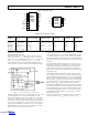


ADM690–ADM695
REV. A
–8–
CE Gating and RAM Write Protection (ADM691/ADM693/
ADM695)
The ADM691/ADM693/ADM695 products include memory
protection circuitry which ensures the integrity of data in mem-
ory by preventing write operations when V
CC
is at an invalid
level. There are two additional pins,
CE
IN
and CE
OUT
, which
may be used to control the Chip Enable or Write inputs of
CMOS RAM. When V
CC
is present, CE
OUT
is a buffered replica
of
CE
IN
, with a 5 ns propagation delay. When V
CC
falls below
the reset voltage threshold or V
BATT
, an internal gate forces
CE
OUT
high, independent of CE
IN
.
CE
OUT
typically drives the CE, CS, or write input of battery
backed up CMOS RAM. This ensures the integrity of the data
in memory by preventing write operations when V
CC
is at an in-
valid level. Similar protection of EEPROMs can be achieved by
using the
CE
OUT
to drive the store or write inputs.
If the 5 ns typical propagation delay of
CE
OUT
is excessive, con-
nect
CE
IN
to GND and use the resulting CE
OUT
to control a
high speed external logic gate.
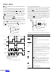
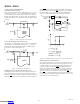
ADM69x
CE
OUT
CE
IN
V
CC
LOW = 0
V
CC
OK = 1
Figure 5. Chip Enable Gating
Power Fail Warning Comparator
An additional comparator is provided for early warning of failure
in the microprocessor’s power supply. The Power Fail Input
(PFI) is compared to an internal +1.3 V reference. The Power
Fail Output (
PFO) goes low when the voltage at PFI is less than
1.3 V. Typically PFI is driven by an external voltage divider
which senses either the unregulated dc input to the system’s 5 V
regulator or the regulated 5 V output. The voltage divider ratio
can be chosen such that the voltage at PFI falls below 1.3 V sev-
eral milliseconds before the +5 V power supply falls below the
reset threshold.
PFO is normally used to interrupt the micropro-
cessor so that data can be stored in RAM and the shut down
procedure executed before power is lost
ADM69x
POWER
FAIL
INPUT
R
2
INPUT
POWER
1.3V
PFO
POWER
FAIL
OUTPUT
R
1
Figure 7. Power Fail Comparator
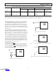
Table II. Input and Output Status In Battery Backup Mode
Signal Status
V
OUT
V
OUT
is connected to V
BATT
via an internal
PMOS switch.
RESET Logic low.
RESET Logic high. The open circuit output voltage is
equal to V
OUT
.
LOW LINE Logic low.
BATT ON Logic high. The open circuit voltage is equal to
V
OUT.
WDI WDI is ignored. It is internally disconnected
from the internal pull-up resistor and does not
source or sink current as long as its input voltage
is between GND and V
OUT
. The input voltage
does not affect supply current.
WDO Logic high. The open circuit voltage is equal
to V
OUT
.
PFI The Power Fail Comparator is turned off and
has no effect on the Power Fail Output.
PFO Logic low.
CE
IN
CE
IN
is ignored. It is internally disconnected
from its internal pull-up and does not source or
sink current as long as its input voltage is
between GND and V
OUT
. The input voltage
does not affect supply current.
CE
OUT
Logic high. The open circuit voltage is equal to
V
OUT
.
OSC IN OSC IN is ignored.
OSC SEL OSC SEL is ignored.
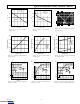
t
1
t
1
= RESET TIME.
V1 = RESET VOLTAGE THRESHOLD LOW
V2 = RESET VOLTAGE THRESHOLD HIGH
HYSTERESIS = V2–V1
V2 V2
V1 V1
t
1
V
CC
LOW LINE
RESET
CE
IN
CE
OUT
Figure 6. Chip Enable Timing
Downloaded from Arrow.com.Downloaded from Arrow.com.Downloaded from Arrow.com.Downloaded from Arrow.com.Downloaded from Arrow.com.Downloaded from Arrow.com.Downloaded from Arrow.com.Downloaded from Arrow.com.