
Datasheet

ADM803/ADM809/ADM810
Rev. H | Page 5 of 12
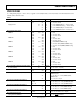
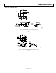
PIN CONFIGURATIONS AND FUNCTION DESCRIPTIONS
GND
1
2
3
ADM803/
ADM809/
1
03736-002
GND
TOP VIEW
(Not to Scale)
V
CC
RESET
Figure 3. ADM803/ADM809 Pin Configuration
2
3
ADM810
TOP VIEW
(Not to Scale)
V
CC
2
RESET
03736-10
Figure 4. ADM810 Pin Configuration
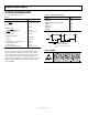
Table 4. Pin Function Descriptions
Pin No.
Mnemonic Description ADM803/ADM809 ADM810
1 1 GND Ground Reference for All Signals; 0 V.
N/A 2 RESET
Active High Logic Output. RESET remains high while V
CC
is below the reset threshold
and remains high for 240 ms (typical) after V
CC
rises above the reset threshold.
2 N/A
RESET Active Low Logic Output. RESET remains low while V
CC
is below the reset threshold
and remains low for 240 ms (typical) after V
CC
rises above the reset threshold.
3 3 V
CC
Supply Voltage Being Monitored.