
Datasheet


Data Sheet ADM811/ADM812
Rev. G | Page 5 of 12
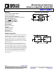
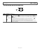
PIN CONFIGURATION AND FUNCTION DESCRIPTIONS
ADM811/
ADM812
TOP VIEW
(Not to Scale)
GND
1
RESET/RESET
2
V
CC
MR
4
3
00092-003
Figure 3. Pin Configuration
Table 3. Pin Function Descriptions
Pin No. Mnemonic Description
1 GND Ground Reference For All Signals, 0 V.
2
RESET
(ADM811)
Active Low Logic Output.
RESET
remains low while V
CC
is below the reset threshold or when
MR
is low;
RESET
then remains low for at least 140 ms (at least 300 ms for the ADM811-3T) after V
CC
rises above the
reset threshold.
RESET (ADM812) Active High Logic Output. RESET remains high while V
CC
is below the reset threshold or when
MR
is low;
RESET then remains high for 240 ms (typical) after V
CC
rises above the reset threshold.
3
MR
Manual Reset. This active low debounced input ignores input pulses of 100 ns or less (typical) and is
guaranteed to accept input pulses of greater than 10 µs. Leave floating when not used.
4 V
CC
Monitored Supply Voltage of 2.5 V, 3 V, 3.3 V, or 5 V. A 0.1 µF decoupling capacitor between V
CC
and the
GND pin is recommended.